IC Package Inspection: Defects, Methods and the Standards Behind Them
Averroes
Nov 19, 2026
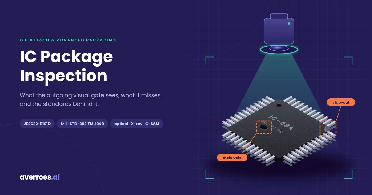
IC package inspection is the visual and automated optical check of finished, packaged chips for mold, marking, terminal and contamination defects before they ship. It runs at the end of assembly and again after reliability stress, against JEDEC JESD22-B101 or MIL-STD-883 Method 2009. External inspection cannot see internal delamination, voids or wire sweep inside the mold body. Those need X-ray or scanning acoustic microscopy.
IC package inspection sits at the end of Stage 07 of the 12-stage semiconductor manufacturing process. This guide from Averroes.ai, an AI visual inspection platform for manufacturers, maps each package defect to the standard that defines it and the method that can catch it.
Key Notes
JESD22-B101D (April 2022) defines external visual inspection of finished packaged devices for qualification, quality monitoring and lot acceptance.
Popcorn cracking starts inside the package: absorbed moisture turns to steam during reflow and delaminates the mold compound before any crack reaches the surface.
JESD22-A113I preconditioning pairs 40x optical inspection with acoustic microscopy, because visual inspection alone misses internal delamination.
Rule-based thresholds at the final visual gate can flag acceptable mold texture and marking variation, sending good parts to manual re-inspection.
What Is IC Package Inspection?
IC package inspection is a back-end quality check that examines finished, packaged integrated circuits for external defects, used to accept or reject devices before shipment and after reliability stress. Here “package” means the chip’s mold body, terminals and marking. It does not mean shipping packaging, and it is not the board-level check covered in PCB visual inspection, which looks at solder joints after the package is mounted.
Package inspection is mostly optical. Optical tools are fast and find surface defects, but they cannot see buried structures, which is why packaging houses add X-ray and acoustic methods for the inside of the package. Semiconductor Engineering reported in December 2019 that no single inspection system meets every packaging requirement, so packaging houses combine several.
Packaged ICs are inspected at five points in the back-end flow:
After molding. Voids, incomplete fill and mold cracks on the package body.
After trim and form or singulation. Bent leads, chip-out at the package edges and dimensional checks.
Final visual before packing. The outgoing gate: a full cosmetic, marking and terminal check against the customer’s procurement specification.
After preconditioning and reliability stress. Cracks, delamination and marking damage after moisture soak, reflow and thermal cycling, including post burn-in visual inspection.
Incoming inspection at the OEM. Sample-based external visual inspection and, for higher-risk parts, X-ray and acoustic checks during incoming component inspection.
The flow shows that external inspection repeats at every hand-off, while internal inspection only appears where the risk justifies the time: qualification, reliability stress and high-reliability incoming checks.
What Defects Does IC Package Inspection Look For?
IC package defects are physical flaws on or inside the mold body, marking, terminals or surfaces of a packaged chip, introduced during molding, marking, trim and form, singulation or handling. Most are visible from the outside. Delamination and wire sweep are not, and they need X-ray or acoustic inspection.
IC package defects: where they form and what sees them
Defect
Package Surface
Typical Origin
Seen By
Risk If Missed
Mold voids, incomplete fill
Body
Molding
Optical, X-ray
Moisture path, cracking
Mold cracks, microcracks
Body
Molding, handling, reflow
Optical, acoustic
Moisture ingress, field failure
Chip-out, edge chipping
Body edges and corners
Singulation, handling
Optical side view
Cracks, loose particles
Exposed wire or copper
Body
Thin mold cap, grinding
Optical
Shorts, corrosion
Foreign material
Any surface
Handling, process residue
Optical
Solderability problems
Marking defects
Top surface
Laser or ink marking
Optical, OCR
Lost traceability
Bent or missing leads
Leads
Trim and form, handling
2D and 3D optical
Opens at board assembly
Poor coplanarity
Leads or balls
Forming, ball attach
3D optical
Opens, weak joints
Ball and pad defects
Bottom surface
Ball attach
3D optical, X-ray
Opens, bridging
Package warpage
Whole body
Material expansion mismatch
3D optical
Weak board joints
Delamination
Internal interfaces
Moisture plus reflow
Acoustic microscopy
Popcorn cracking, bond damage
Wire sweep
Internal wires
Mold flow
X-ray
Shorts between wires
Chip-out at singulation can open a moisture path into the package, so an edge chip that looks cosmetic can become a reliability defect after reflow. Package chip-out is a different defect from die-edge chipping during wafer dicing, which happens before the die is ever packaged. Methods for finding and sizing package cracks are covered in the crack inspection guide.
The atlas makes one point: almost every external defect class sits on a different surface, which is why automated package inspection images each package from several sides.
Which Standards Define External Visual Inspection of IC Packages?
External visual inspection (EVI) is a noninvasive, nondestructive test method that examines the surfaces, construction, marking and workmanship of a finished packaged device, used for qualification, quality monitoring and lot acceptance. That scope comes from JEDEC JESD22-B101D, published in April 2022. The method excludes internal features that cannot be seen, and it does not apply to piece parts still in assembly.
IC package inspection standards compared
Standard
Scope
Applies To
When It Is Used
JESD22-B101D (JEDEC, April 2022)
External visual inspection
Finished packaged devices, all package types
Qualification, quality monitoring, lot acceptance
MIL-STD-883, Test Method 2009
External visual workmanship
Hermetically packaged microcircuits
High-reliability screening and qualification
JESD22-A113I (JEDEC, April 2020)
Preconditioning before reliability tests
Non-hermetic surface mount devices
Before humidity, bias and thermal cycling tests
J-STD-020F (IPC/JEDEC, December 2022)
Moisture and reflow sensitivity classification
Non-hermetic surface mount devices
Assigning a moisture sensitivity level
J-STD-035 (IPC/JEDEC)
Acoustic microscopy
Non-hermetic encapsulated components
Detecting internal delamination
JESD22-B108B (JEDEC, 2010, reaffirmed 2023)
Terminal coplanarity at room temperature
Surface mount devices
Inspection and device characterization
JESD22-B112 (JEDEC)
Package warpage at elevated temperature
Surface mount ICs
Warpage across the reflow profile
Commercial plastic packages are usually inspected to JESD22-B101 inside a JEDEC qualification flow. Hermetic and high-reliability parts are inspected to MIL-STD-883 Method 2009, and MIL-PRF-38535 requires 100% external visual inspection for Class B and Class S devices (Infineon MIL-PRF-38535 summary, accessed November 2026).
JESD22-A113I (April 2020) specifies an optical microscope at 40x for the external visual exam during preconditioning. Magnification and accept limits in production come from the procurement document built on the standard, not from the standard alone.
What Package Defects Can External Inspection Not See?
Internal package defects are delaminations, voids, cracks and interconnect faults beneath the mold surface that external visual inspection cannot detect, and that require X-ray or acoustic inspection. The mold compound is opaque to light, so an optical system sees only the outer surface of the package.
The most common internal failure starts with moisture. A plastic package absorbs moisture from the air. During reflow soldering, that moisture turns to steam, which separates the mold compound from the die or lead frame. In severe cases the pressure cracks the package from the inside out. External inspection sees only that last stage.
What Is Popcorn Cracking?
Popcorn cracking is a package failure mode in which moisture absorbed by a plastic IC package vaporizes during solder reflow and cracks the package, used as a name for the most severe form of moisture-induced damage. A NAVSEA microcircuit handling guide describes the sequence: internal delamination and cracks first, then bond damage, then in the worst case an external crack that can make an audible pop.
IPC/JEDEC J-STD-020F (December 2022) classifies each non-hermetic surface mount device into a moisture sensitivity level, which sets how long it can sit on the factory floor before reflow. IPC/JEDEC J-STD-033 sets the matching handling, packing, shipping and baking rules. Preconditioning to these levels is part of semiconductor reliability testing.
How Is Package Delamination Detected?
Scanning acoustic microscopy (C-SAM) is a nondestructive imaging method that sends ultrasound through a package and maps the echoes from internal interfaces, used to find delamination, cracks and voids inside plastic packages. A delamination is a thin air gap, and air reflects almost all of the acoustic signal, which makes it stand out clearly in an acoustic image. A 2014 NASA technical report calls acoustic micro-imaging the preferred method for air gaps such as delamination, cracks, voids and porosity.
X-ray works differently. It images density, so it is strong on voids, wire sweep, bond wires and solder joints but cannot distinguish a delaminated interface. J-STD-035 covers acoustic microscopy of non-hermetic components, and J-STD-020 runs acoustic microscopy before and after reflow during moisture sensitivity classification. X-ray methods for packages are covered in automated X-ray inspection.
What each inspection method sees inside and outside an IC package
Method
What It Sees
What It Misses
2D optical
Surface defects, marking, contamination
Anything below the mold surface
3D optical
Coplanarity, standoff, warpage
Internal interfaces
X-ray (2D and CT)
Voids, wire sweep, bond wires, solder joints
Thin delamination air gaps
Acoustic microscopy (C-SAM)
Delamination, internal cracks, voids
Some solder joint failures in area-array assemblies
The cross-section shows why the methods are complementary: each one sees a different layer of the same package, and none sees all of them.
How Do Automated IC Package Inspection Systems Work?
Automated package inspection is a machine vision process that images each packaged IC from several sides under controlled lighting and measures it against dimensional and cosmetic limits, used to sort devices at line speed. Semiconductor Engineering reported in December 2019 that optical inspection is the main production method in packaging houses.
A typical automated package inspection system runs four checks:
2D imaging of every surface. Top, bottom and the four sides, often called five-side or six-side inspection, to find mold, marking and contamination defects.
3D measurement of terminals and body. Lead and ball coplanarity, standoff and package warpage, following the seating-plane method in JESD22-B108B.
Marking verification. Optical character reading of the part number, lot code and orientation mark.
Sort and output. Passing parts go to automated tray inspection or tape and reel. Rejects go to a review bin.
KLA’s ICOS T3/T7 and T890XP systems are examples of this category, inspecting packaged ICs with tray or tape output and, on the T890XP, singulated substrates. The same imaging principles are described for general manufacturing in automated visual inspection systems. Advanced packages add finer features and new defect types, covered in advanced packaging metrology.
The weak point is the decision, not the image. Plastic mold compound has natural texture, laser marks vary in contrast, and glossy surfaces create glare. A fixed threshold cannot always tell those from a real void or chip-out, so it over-rejects. Separating real defects from acceptable variation is a job for AI defect classification.
How Does AI Reduce False Rejects at the Package Inspection Gate?
AI defect review is software that re-examines the images behind each automated reject and separates real package defects from acceptable cosmetic variation, used to cut manual re-inspection without loosening inspection limits. It sits between the inspection system’s reject decision and the operator who confirms it.
The outgoing gate has a built-in trade-off. Tight thresholds catch more real defects but reject more good parts, which then go to manual re-inspection or scrap. Loose thresholds pass more good parts but let real defects escape to the customer. AI review breaks that trade: the inspection system stays at full sensitivity, and a trained model decides which rejects are real. The difference from rule-based thresholds is covered in automatic defect classification.
The same problem appears at two gates:
Final visual inspection at the OSAT or IDM. Every package is imaged before shipping. Over-rejection costs re-inspection labor and yield.
Incoming inspection at the OEM. Sampled packages are inspected against the procurement specification, and the same cosmetic ambiguity applies. External visual inspection is also part of counterfeit semiconductor detection, where surface and marking detail matters.
Averroes.ai is an AI visual inspection platform built to run as an overlay on the inspection systems a site already owns, not to replace them. It trains classification models from 20 to 40 labeled images per defect class, with no code, and deploys on premise so package image data stays inside the customer environment. Trending classified rejects by lot, mold tool and package type with defect monitoring turns a recurring cosmetic reject into a process fix at the molding or trim and form step.
Good Parts Stuck in Manual Re-Inspection?
Test AI defect review on your own package reject images
Frequently Asked Questions
What is external visual inspection of a semiconductor package?
External visual inspection of a semiconductor package is the JEDEC JESD22-B101 test method that examines a finished device’s surfaces, construction, marking and workmanship without damaging it. It is used for qualification, quality monitoring and lot acceptance. Hermetic and high-reliability parts use MIL-STD-883 Method 2009 instead.
What magnification is used for IC package visual inspection?
JEDEC JESD22-A113I (April 2020) specifies an optical microscope at 40x for the external visual exam during preconditioning. Production magnification and accept limits are set in the procurement document that applies the standard, so they vary by customer, package type and reliability class.
What is popcorn cracking in IC packages?
Popcorn cracking is a failure where moisture absorbed by a plastic IC package turns to steam during solder reflow and cracks the package from the inside. It starts as internal delamination that external inspection cannot see. IPC/JEDEC J-STD-020F moisture sensitivity levels and J-STD-033 handling rules exist to prevent it.
Can X-ray inspection find package delamination?
X-ray inspection generally cannot find package delamination, because X-ray images density and a delamination is a thin air gap between two layers. Scanning acoustic microscopy (C-SAM) is the standard method for delamination. X-ray is the right tool for voids, wire sweep, bond wires and solder joints inside the package.
What is lead coplanarity in IC packages?
Lead coplanarity is how far each lead or solder ball of a surface mount package sits from the seating plane formed by the lowest terminals. JEDEC JESD22-B108B measures it at room temperature. Poor coplanarity causes open or weak joints when the package is soldered to a board.
How is IC package inspection different from PCB inspection?
IC package inspection checks the component itself before it is mounted: mold body, marking, leads and balls. PCB inspection checks the assembled board after soldering: placement, solder joints and bridges. A package that passes inspection can still fail at board level if warpage or coplanarity causes poor joints.






IC package inspection is the visual and automated optical check of finished, packaged chips for mold, marking, terminal and contamination defects before they ship. It runs at the end of assembly and again after reliability stress, against JEDEC JESD22-B101 or MIL-STD-883 Method 2009. External inspection cannot see internal delamination, voids or wire sweep inside the mold body. Those need X-ray or scanning acoustic microscopy.
IC package inspection sits at the end of Stage 07 of the 12-stage semiconductor manufacturing process. This guide from Averroes.ai, an AI visual inspection platform for manufacturers, maps each package defect to the standard that defines it and the method that can catch it.
Key Notes
What Is IC Package Inspection?
IC package inspection is a back-end quality check that examines finished, packaged integrated circuits for external defects, used to accept or reject devices before shipment and after reliability stress. Here “package” means the chip’s mold body, terminals and marking. It does not mean shipping packaging, and it is not the board-level check covered in PCB visual inspection, which looks at solder joints after the package is mounted.
Package inspection is mostly optical. Optical tools are fast and find surface defects, but they cannot see buried structures, which is why packaging houses add X-ray and acoustic methods for the inside of the package. Semiconductor Engineering reported in December 2019 that no single inspection system meets every packaging requirement, so packaging houses combine several.
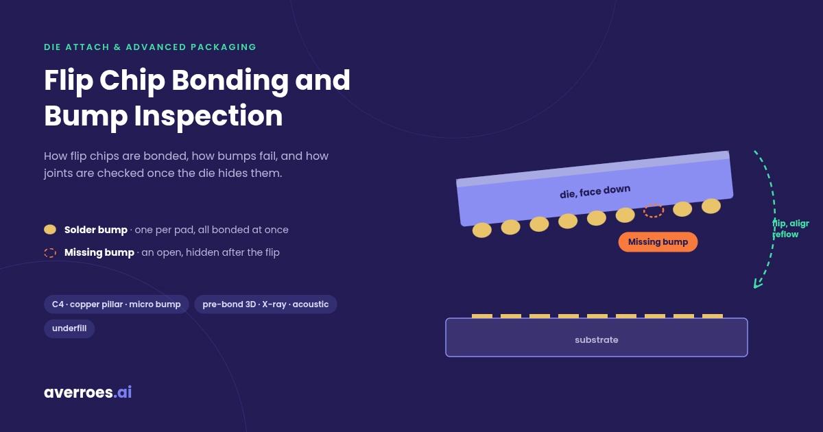
By the time a chip reaches package inspection, its die has already passed wafer test as a known good die and been connected by wire bonding or flip chip bonding inside the die attach and advanced packaging stage.
Packaged ICs are inspected at five points in the back-end flow:
The flow shows that external inspection repeats at every hand-off, while internal inspection only appears where the risk justifies the time: qualification, reliability stress and high-reliability incoming checks.
What Defects Does IC Package Inspection Look For?
IC package defects are physical flaws on or inside the mold body, marking, terminals or surfaces of a packaged chip, introduced during molding, marking, trim and form, singulation or handling. Most are visible from the outside. Delamination and wire sweep are not, and they need X-ray or acoustic inspection.
IC package defects: where they form and what sees them
Chip-out at singulation can open a moisture path into the package, so an edge chip that looks cosmetic can become a reliability defect after reflow. Package chip-out is a different defect from die-edge chipping during wafer dicing, which happens before the die is ever packaged. Methods for finding and sizing package cracks are covered in the crack inspection guide.
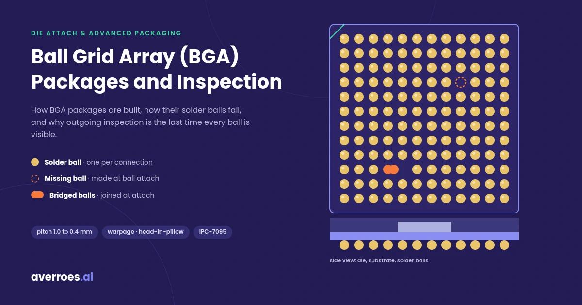
Marking defects get a full treatment in laser mark inspection, and ball and pad defects on area-array packages in the ball grid array guide.
The atlas makes one point: almost every external defect class sits on a different surface, which is why automated package inspection images each package from several sides.
Which Standards Define External Visual Inspection of IC Packages?
External visual inspection (EVI) is a noninvasive, nondestructive test method that examines the surfaces, construction, marking and workmanship of a finished packaged device, used for qualification, quality monitoring and lot acceptance. That scope comes from JEDEC JESD22-B101D, published in April 2022. The method excludes internal features that cannot be seen, and it does not apply to piece parts still in assembly.
IC package inspection standards compared
Commercial plastic packages are usually inspected to JESD22-B101 inside a JEDEC qualification flow. Hermetic and high-reliability parts are inspected to MIL-STD-883 Method 2009, and MIL-PRF-38535 requires 100% external visual inspection for Class B and Class S devices (Infineon MIL-PRF-38535 summary, accessed November 2026).
JESD22-A113I (April 2020) specifies an optical microscope at 40x for the external visual exam during preconditioning. Magnification and accept limits in production come from the procurement document built on the standard, not from the standard alone.
What Package Defects Can External Inspection Not See?
Internal package defects are delaminations, voids, cracks and interconnect faults beneath the mold surface that external visual inspection cannot detect, and that require X-ray or acoustic inspection. The mold compound is opaque to light, so an optical system sees only the outer surface of the package.
The most common internal failure starts with moisture. A plastic package absorbs moisture from the air. During reflow soldering, that moisture turns to steam, which separates the mold compound from the die or lead frame. In severe cases the pressure cracks the package from the inside out. External inspection sees only that last stage.
What Is Popcorn Cracking?
Popcorn cracking is a package failure mode in which moisture absorbed by a plastic IC package vaporizes during solder reflow and cracks the package, used as a name for the most severe form of moisture-induced damage. A NAVSEA microcircuit handling guide describes the sequence: internal delamination and cracks first, then bond damage, then in the worst case an external crack that can make an audible pop.
IPC/JEDEC J-STD-020F (December 2022) classifies each non-hermetic surface mount device into a moisture sensitivity level, which sets how long it can sit on the factory floor before reflow. IPC/JEDEC J-STD-033 sets the matching handling, packing, shipping and baking rules. Preconditioning to these levels is part of semiconductor reliability testing.
How Is Package Delamination Detected?
Scanning acoustic microscopy (C-SAM) is a nondestructive imaging method that sends ultrasound through a package and maps the echoes from internal interfaces, used to find delamination, cracks and voids inside plastic packages. A delamination is a thin air gap, and air reflects almost all of the acoustic signal, which makes it stand out clearly in an acoustic image. A 2014 NASA technical report calls acoustic micro-imaging the preferred method for air gaps such as delamination, cracks, voids and porosity.
X-ray works differently. It images density, so it is strong on voids, wire sweep, bond wires and solder joints but cannot distinguish a delaminated interface. J-STD-035 covers acoustic microscopy of non-hermetic components, and J-STD-020 runs acoustic microscopy before and after reflow during moisture sensitivity classification. X-ray methods for packages are covered in automated X-ray inspection.
What each inspection method sees inside and outside an IC package
The cross-section shows why the methods are complementary: each one sees a different layer of the same package, and none sees all of them.
How Do Automated IC Package Inspection Systems Work?
Automated package inspection is a machine vision process that images each packaged IC from several sides under controlled lighting and measures it against dimensional and cosmetic limits, used to sort devices at line speed. Semiconductor Engineering reported in December 2019 that optical inspection is the main production method in packaging houses.
A typical automated package inspection system runs four checks:
KLA’s ICOS T3/T7 and T890XP systems are examples of this category, inspecting packaged ICs with tray or tape output and, on the T890XP, singulated substrates. The same imaging principles are described for general manufacturing in automated visual inspection systems. Advanced packages add finer features and new defect types, covered in advanced packaging metrology.
The weak point is the decision, not the image. Plastic mold compound has natural texture, laser marks vary in contrast, and glossy surfaces create glare. A fixed threshold cannot always tell those from a real void or chip-out, so it over-rejects. Separating real defects from acceptable variation is a job for AI defect classification.
How Does AI Reduce False Rejects at the Package Inspection Gate?
AI defect review is software that re-examines the images behind each automated reject and separates real package defects from acceptable cosmetic variation, used to cut manual re-inspection without loosening inspection limits. It sits between the inspection system’s reject decision and the operator who confirms it.
The outgoing gate has a built-in trade-off. Tight thresholds catch more real defects but reject more good parts, which then go to manual re-inspection or scrap. Loose thresholds pass more good parts but let real defects escape to the customer. AI review breaks that trade: the inspection system stays at full sensitivity, and a trained model decides which rejects are real. The difference from rule-based thresholds is covered in automatic defect classification.
The same problem appears at two gates:
Averroes.ai is an AI visual inspection platform built to run as an overlay on the inspection systems a site already owns, not to replace them. It trains classification models from 20 to 40 labeled images per defect class, with no code, and deploys on premise so package image data stays inside the customer environment. Trending classified rejects by lot, mold tool and package type with defect monitoring turns a recurring cosmetic reject into a process fix at the molding or trim and form step.
Good Parts Stuck in Manual Re-Inspection?
Test AI defect review on your own package reject images
Frequently Asked Questions
What is external visual inspection of a semiconductor package?
External visual inspection of a semiconductor package is the JEDEC JESD22-B101 test method that examines a finished device’s surfaces, construction, marking and workmanship without damaging it. It is used for qualification, quality monitoring and lot acceptance. Hermetic and high-reliability parts use MIL-STD-883 Method 2009 instead.
What magnification is used for IC package visual inspection?
JEDEC JESD22-A113I (April 2020) specifies an optical microscope at 40x for the external visual exam during preconditioning. Production magnification and accept limits are set in the procurement document that applies the standard, so they vary by customer, package type and reliability class.
What is popcorn cracking in IC packages?
Popcorn cracking is a failure where moisture absorbed by a plastic IC package turns to steam during solder reflow and cracks the package from the inside. It starts as internal delamination that external inspection cannot see. IPC/JEDEC J-STD-020F moisture sensitivity levels and J-STD-033 handling rules exist to prevent it.
Can X-ray inspection find package delamination?
X-ray inspection generally cannot find package delamination, because X-ray images density and a delamination is a thin air gap between two layers. Scanning acoustic microscopy (C-SAM) is the standard method for delamination. X-ray is the right tool for voids, wire sweep, bond wires and solder joints inside the package.
What is lead coplanarity in IC packages?
Lead coplanarity is how far each lead or solder ball of a surface mount package sits from the seating plane formed by the lowest terminals. JEDEC JESD22-B108B measures it at room temperature. Poor coplanarity causes open or weak joints when the package is soldered to a board.
How is IC package inspection different from PCB inspection?
IC package inspection checks the component itself before it is mounted: mold body, marking, leads and balls. PCB inspection checks the assembled board after soldering: placement, solder joints and bridges. A package that passes inspection can still fail at board level if warpage or coplanarity causes poor joints.