Wire Bonding: How Wire Bonds Are Made, How They Fail and How They Are Inspected
Averroes
Nov 14, 2026
Wire bonding connects a chip’s bond pads to its package with fine gold, copper or aluminum wire, and it is used to assemble the vast majority of semiconductor packages. Ball bonding, about 90% of bonds, welds a melted wire ball to the pad; wedge bonding presses the wire flat. Wire bonds fail as non-sticks, lifted bonds, heel cracks and wire sweep, which AI visual inspection platforms such as Averroes.ai help classify before molding.
Wire bonding sits in Stage 07 of the semiconductor manufacturing process, after die attach and before molding. This guide covers how wire bonds are made, the defects that matter, where each one can be caught, and how bonds are tested.
Key Notes
Ball bonding dominates: about 90% of packages use ball bonds and about 10% wedge bonds, according to patent literature.
Copper is replacing gold: it costs less, but it is harder, so bonding parameters need tighter control.
Some defects start before bonding: a Peregrine Semiconductor study traced non-stick on pad to bond pad contamination.
Molding hides wire defects: wire sweep can appear only after encapsulation, where X-ray, not optics, can see it.
What Is Wire Bonding?
Wire bonding is an interconnect process that welds fine metal wire between a die’s bond pads and its package leads or substrate, used to carry signals and power out of the chip. It is generally considered the most cost-effective and flexible interconnect technology and is used to assemble the vast majority of semiconductor packages.
In the assembly flow, wire bonding comes after die attach, which fixes the die in the package, and before molding, which seals the die and wires in compound. The dies arriving at the bonder should already be known good die, screened by test and inspection, because a bad die bonded into a package wastes the package too. Wire bonding sits in the die attach and advanced packaging stage of the hub, alongside the newer interconnects covered in advanced packaging metrology.
“Wire bonding” here means semiconductor packaging, not the construction wire anchors that share the name in search results. It is also different from die bonding, which attaches the die itself, and from wafer or hybrid bonding, which joins whole wafers or dies face to face.
How Does the Wire Bonding Process Work?
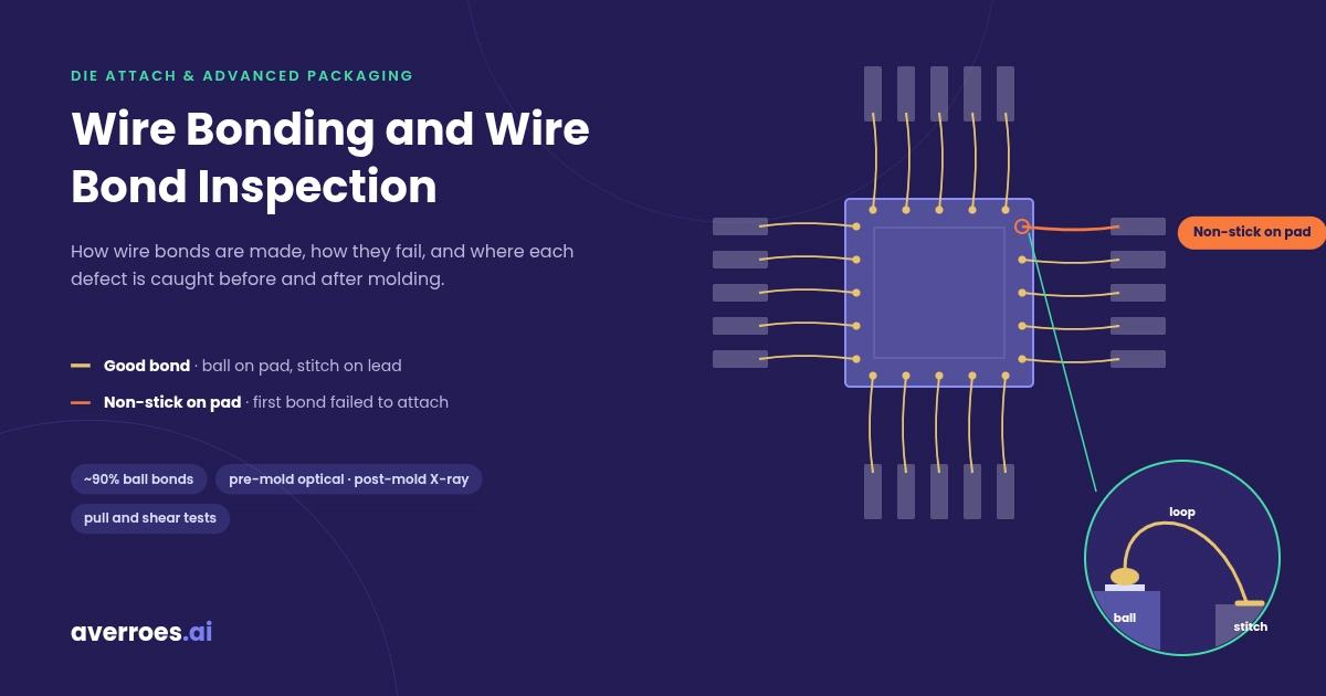
The wire bonding process is a repeated bonding cycle that forms one wire connection at a time, used to link every pad on the die to its matching lead. In ball bonding, the most common form, each wire is made in five steps:
Form the free air ball. An electronic flame-off (EFO) spark melts the wire tip into a small ball at the end of the capillary.
Make the first bond. The capillary presses the ball onto the die’s bond pad, and heat, force and ultrasonic energy weld it in place.
Form the loop. The capillary rises and moves toward the lead, shaping the wire into a controlled loop.
Make the second bond. The capillary presses the wire onto the lead, forming a flat crescent or stitch bond.
Tear the tail. The wire clamps close and the capillary rises, breaking the wire and leaving enough tail to form the next ball.
Semiconductor Digest’s wire bonding fundamentals describe this cycle, ending with the flame-off forming a new free air ball for the next wire.
What Is the Difference Between Ball Bonding and Wedge Bonding?
Ball bonding is a bonding method that welds a melted wire ball to the first pad, used for most fine-pitch IC packages; wedge bonding is a method that presses the wire flat with a wedge-shaped tool, used for aluminum wire and power devices. Patent literature puts the split at about 90% of packages using ball bonds and about 10% using wedge bonds.
Ball bonding vs wedge bonding
Factor
Ball Bonding
Wedge Bonding
First bond shape
Melted ball on the pad
Wire pressed flat
Typical wire
Gold or copper
Aluminum, also gold or copper
Heat
Usually needed
Aluminum and copper at room temperature
Direction
Wire can leave in any direction
Wire must follow the first bond’s direction
Speed
Faster
Slower, tool must rotate
Typical use
Most IC packages
Power devices, large wire or ribbon
Wedge bonding is slower because the tool is directional: the wire must leave the first bond in a straight line, so the bond head turns between wires. Ball bonding has no preferred direction, which makes it faster. Wedge bonding’s strength is large wire and ribbon for power electronics.
Which Wire Materials Are Used?
Bonding wire is a high-purity metal wire chosen for conductivity, cost and how it bonds, used in diameters from tens of micrometers up to large power wire. Three materials dominate:
Gold was the long-standing standard for ball bonding.
Copper is replacing gold because of gold’s rising cost and copper’s lower, more stable price. Copper is harder than gold and aluminum, so bonding parameters must be kept under tight control. Patent literature also notes copper’s resistance to wire sweep.
Aluminum is used mainly for wedge bonding, including large wire for power devices.
The takeaway: the bond type and wire material set which defects are most likely, and so what inspection must look for.
What Are the Most Common Wire Bond Defects?
A wire bond defect is a flaw in the bond or the wire that weakens or breaks the connection, used in assembly as the reject criteria before molding. The most common ones form during bonding itself or during the molding step that follows.
Wire bond defects and where they come from
Defect
What It Is
Typical Causes
When It Can Be Caught
Non-stick on pad (NSOP)
First bond fails to attach
Bond pad contamination
During bonding, pre-mold optical
Lifted ball
Ball separates from the pad
Contamination, wrong settings, corrosion, probing
Pre-mold optical, ball shear
Heel crack
Crack at the second bond’s heel
Microcrack formed during bonding
High-magnification optical, pull test
Wire sweep
Wires pushed out of position
Mold compound flow
Post-mold X-ray
Sagging or sway
Loop out of shape
Looping settings
Pre-mold optical
Cratering
Damage under the bond pad
Excess bonding force or energy
Destructive cratering test
Shorts
Wires touching
Sweep, sagging, loop errors
Optical or X-ray
Sources: defect causes from the Peregrine NSOP study, Knowles’ ball shear application note and a published wire bond quality test review; wire sweep after molding from Viasion’s process overview.
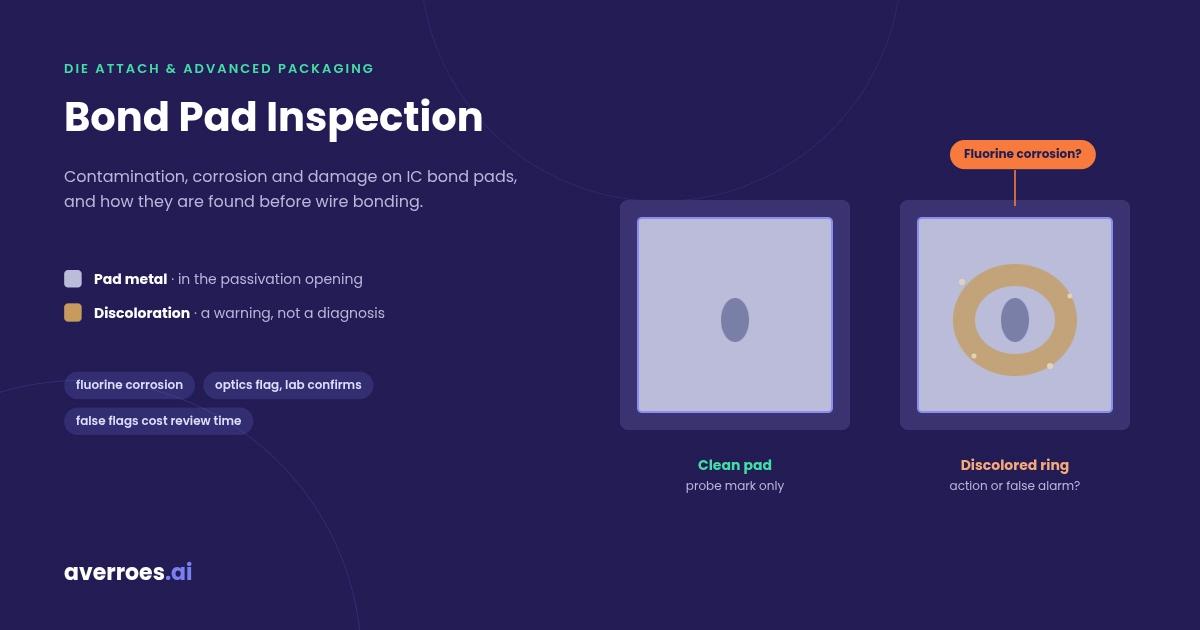
Some causes come from the bonder: wrong bond force, ultrasonic energy or loop settings. Others come from upstream. Knowles’ application note lists contamination on the bond pad, pad corrosion and excessive bond pad probing among the causes of ball lifting, which links bonding quality back to the probe marks covered in probe mark inspection.
What Causes Non-Stick on Pad?
Non-stick on pad (NSOP) is a bonding defect in which the first bond fails to attach to the die’s bond pad, used as a key yield measure on wire bond lines because it leaves an open connection. Bonders can flag some non-sticks electrically during bonding, by checking continuity through the wire, as patent literature on non-stick detection describes.
The cause is often not the bonder. In a Peregrine Semiconductor study presented through IPC, engineers isolated the dies showing NSOP, mapped them, and confirmed through process mapping that the root cause was bond pad contamination. They then added automated optical inspection at the wafer back end to isolate and root-cause these defects before assembly, and outgoing defect rates dropped. The bond failed at bonding, but the problem was on the pad before the wire ever arrived. Pad condition is covered in bond pad inspection.
Once a package is molded, a bad bond is sealed in. Catching pad and bond defects before molding is where inspection pays for itself.
Catch Bond Defects Before Mold Hides Them
Test AI defect review on your own wire bond images
The takeaway: some wire bond defects are made at the bonder, and some arrive with the pad.
Which Inspection Methods Detect Wire Bond Defects?
Wire bond inspection is the check of bonds and wire loops for position, shape and attachment, used to stop defective units before molding and to confirm wire integrity after it. No single method sees every defect, because molding changes what is visible.
Before molding, optical inspection looks down on the bonds and loops. Viasion’s process overview describes it as manual, sampled or 100%, or automated, checking for wire shorts, non-sticking and lifted wires. MIL-STD-883 Method 2010 sets internal visual inspection criteria for high-reliability parts. Imaging and processing methods for this kind of inspection are covered in die inspection.
After molding, optics cannot see through the compound. Wire sweep can appear only after molding, so lines use X-ray to check that wires stayed in position, along with shorts and broken or missing wires. X-ray methods are covered in automated X-ray inspection, and the outside of the finished package in IC package cosmetic inspection.
The two are complementary. Optical inspection sees the pad surface and bond shape but not the inside of a molded package; X-ray sees the wires inside but not the surface condition of the pad.
The takeaway: inspect before molding for what X-ray cannot see, and after molding for what optics cannot reach.
How Are Wire Bonds Tested?
Wire bond testing is the destructive measurement of bond strength on sample units, used in process qualification and process control alongside 100% inspection. Two tests dominate.
What Is a Wire Pull Test?
A wire pull test is a destructive test that hooks the wire and pulls until it breaks, used to measure bond strength and record where the bond failed. MIL-STD-883 Method 2011 defines the method: it measures bond strengths and their distribution, pulls at 90 degrees unless otherwise specified, records the failure force and failure category, and is performed before any encapsulant that would raise the apparent strength. ASTM F458 covers non-destructive pull testing, which stresses the bond to a set force without breaking good bonds.
What Is a Ball Shear Test?
A ball shear test is a destructive test that pushes a chisel against the side of a ball bond, used to measure how strongly the ball holds to the pad. JEDEC JESD22-B116B, revised in April 2017, defines it for ball bonds made with wire from 15 µm to 76 µm, before or after encapsulation. The standard notes that shear testing of wedge bonds has not been shown to be a consistent indicator of bond integrity.
Both tests destroy the bonds they measure, so they run on samples. Inspection is what covers every unit. Wider reliability testing of packages is covered in semiconductor bonding reliability testing.
Where Does AI Fit in Wire Bond Inspection?
AI wire bond inspection is image-based classification that sorts bond and loop images into real defect classes and acceptable variation, used to make 100% pre-mold inspection practical without flooding reviewers. Wire bonds vary in shape from unit to unit even when they are good, which is what makes rule-based inspection noisy.
AI does four jobs in wire bond inspection:
Classify pre-mold images into NSOP, lifted ball, heel crack, sagging and shorts, and separate them from acceptable shape variation.
Route borderline units to review with the classification attached, so an engineer confirms the call.
Trend defects by bonder, capillary and lot, so a worn capillary or drifting setting shows up before it fills a lot with rejects.
Tie bond defects back to the pad, so a rise in non-sticks can be checked against bond pad inspection results upstream.
Averroes.ai runs AI defect review and AI defect classification on the optical images a wire bond line already captures. It trains from 20 to 40 labeled images per defect class, with no code, and deploys on premise. Averroes is not a wire bonder, pull tester or X-ray system: it works on the images those tools produce. You can test AI defect review on your own wire bond images.
Frequently Asked Questions
What is the difference between ball bonding and wedge bonding?
Ball bonding melts the wire tip into a ball and welds it to the pad, and the wire can leave in any direction, which makes it fast. Wedge bonding presses the wire flat with a wedge tool and must follow the bond’s direction. About 90% of packages use ball bonds, and wedge bonding suits aluminum and power devices.
Why is copper replacing gold in wire bonding?
Copper costs much less than gold, and its price is more stable, so the industry has been moving from gold to copper bonding wire. Copper is harder than gold and aluminum, though, so bonding parameters must be controlled tightly to avoid damaging the pad. Patent literature also notes copper’s resistance to wire sweep.
What is non-stick on pad (NSOP)?
Non-stick on pad is a wire bonding defect in which the first bond fails to attach to the die’s bond pad, leaving an open connection. Bonders can flag some non-sticks electrically. A Peregrine Semiconductor study traced NSOP to bond pad contamination, so pad inspection before bonding helps prevent it.
What is wire sweep?
Wire sweep is a defect in which bond wires are pushed out of position, often by the flow of mold compound during encapsulation. Swept wires can touch and short. Because it can appear only after molding, optical inspection cannot see it, and lines use X-ray inspection to check wire position inside the package.
What is a wire pull test?
A wire pull test hooks a bond wire and pulls until it breaks, recording the force and where the failure happened. MIL-STD-883 Method 2011 defines the destructive version, pulling at 90 degrees unless specified. It runs on samples during process qualification and control, because it destroys the bonds it tests.
Can wire bond defects be seen after molding?
Partly. Mold compound blocks optical inspection, so surface defects such as non-sticks or lifted balls must be caught before molding. After molding, X-ray inspection can still see wire position, sweep, shorts and broken or missing wires inside the package, but not the condition of the bond pad surface.






Wire bonding connects a chip’s bond pads to its package with fine gold, copper or aluminum wire, and it is used to assemble the vast majority of semiconductor packages. Ball bonding, about 90% of bonds, welds a melted wire ball to the pad; wedge bonding presses the wire flat. Wire bonds fail as non-sticks, lifted bonds, heel cracks and wire sweep, which AI visual inspection platforms such as Averroes.ai help classify before molding.
Wire bonding sits in Stage 07 of the semiconductor manufacturing process, after die attach and before molding. This guide covers how wire bonds are made, the defects that matter, where each one can be caught, and how bonds are tested.
Key Notes
What Is Wire Bonding?
Wire bonding is an interconnect process that welds fine metal wire between a die’s bond pads and its package leads or substrate, used to carry signals and power out of the chip. It is generally considered the most cost-effective and flexible interconnect technology and is used to assemble the vast majority of semiconductor packages.
In the assembly flow, wire bonding comes after die attach, which fixes the die in the package, and before molding, which seals the die and wires in compound. The dies arriving at the bonder should already be known good die, screened by test and inspection, because a bad die bonded into a package wastes the package too. Wire bonding sits in the die attach and advanced packaging stage of the hub, alongside the newer interconnects covered in advanced packaging metrology.
“Wire bonding” here means semiconductor packaging, not the construction wire anchors that share the name in search results. It is also different from die bonding, which attaches the die itself, and from wafer or hybrid bonding, which joins whole wafers or dies face to face.
How Does the Wire Bonding Process Work?
The wire bonding process is a repeated bonding cycle that forms one wire connection at a time, used to link every pad on the die to its matching lead. In ball bonding, the most common form, each wire is made in five steps:
Semiconductor Digest’s wire bonding fundamentals describe this cycle, ending with the flame-off forming a new free air ball for the next wire.
What Is the Difference Between Ball Bonding and Wedge Bonding?
Ball bonding is a bonding method that welds a melted wire ball to the first pad, used for most fine-pitch IC packages; wedge bonding is a method that presses the wire flat with a wedge-shaped tool, used for aluminum wire and power devices. Patent literature puts the split at about 90% of packages using ball bonds and about 10% using wedge bonds.
Ball bonding vs wedge bonding
Wedge bonding is slower because the tool is directional: the wire must leave the first bond in a straight line, so the bond head turns between wires. Ball bonding has no preferred direction, which makes it faster. Wedge bonding’s strength is large wire and ribbon for power electronics.
Which Wire Materials Are Used?
Bonding wire is a high-purity metal wire chosen for conductivity, cost and how it bonds, used in diameters from tens of micrometers up to large power wire. Three materials dominate:
The takeaway: the bond type and wire material set which defects are most likely, and so what inspection must look for.
What Are the Most Common Wire Bond Defects?
A wire bond defect is a flaw in the bond or the wire that weakens or breaks the connection, used in assembly as the reject criteria before molding. The most common ones form during bonding itself or during the molding step that follows.
Wire bond defects and where they come from
Sources: defect causes from the Peregrine NSOP study, Knowles’ ball shear application note and a published wire bond quality test review; wire sweep after molding from Viasion’s process overview.
Some causes come from the bonder: wrong bond force, ultrasonic energy or loop settings. Others come from upstream. Knowles’ application note lists contamination on the bond pad, pad corrosion and excessive bond pad probing among the causes of ball lifting, which links bonding quality back to the probe marks covered in probe mark inspection.
What Causes Non-Stick on Pad?
Non-stick on pad (NSOP) is a bonding defect in which the first bond fails to attach to the die’s bond pad, used as a key yield measure on wire bond lines because it leaves an open connection. Bonders can flag some non-sticks electrically during bonding, by checking continuity through the wire, as patent literature on non-stick detection describes.
The cause is often not the bonder. In a Peregrine Semiconductor study presented through IPC, engineers isolated the dies showing NSOP, mapped them, and confirmed through process mapping that the root cause was bond pad contamination. They then added automated optical inspection at the wafer back end to isolate and root-cause these defects before assembly, and outgoing defect rates dropped. The bond failed at bonding, but the problem was on the pad before the wire ever arrived. Pad condition is covered in bond pad inspection.
Once a package is molded, a bad bond is sealed in. Catching pad and bond defects before molding is where inspection pays for itself.
Catch Bond Defects Before Mold Hides Them
Test AI defect review on your own wire bond images
The takeaway: some wire bond defects are made at the bonder, and some arrive with the pad.
Which Inspection Methods Detect Wire Bond Defects?
Wire bond inspection is the check of bonds and wire loops for position, shape and attachment, used to stop defective units before molding and to confirm wire integrity after it. No single method sees every defect, because molding changes what is visible.
Where each wire bond defect is caught
Before molding, optical inspection looks down on the bonds and loops. Viasion’s process overview describes it as manual, sampled or 100%, or automated, checking for wire shorts, non-sticking and lifted wires. MIL-STD-883 Method 2010 sets internal visual inspection criteria for high-reliability parts. Imaging and processing methods for this kind of inspection are covered in die inspection.
After molding, optics cannot see through the compound. Wire sweep can appear only after molding, so lines use X-ray to check that wires stayed in position, along with shorts and broken or missing wires. X-ray methods are covered in automated X-ray inspection, and the outside of the finished package in IC package cosmetic inspection.
The two are complementary. Optical inspection sees the pad surface and bond shape but not the inside of a molded package; X-ray sees the wires inside but not the surface condition of the pad.
The takeaway: inspect before molding for what X-ray cannot see, and after molding for what optics cannot reach.
How Are Wire Bonds Tested?
Wire bond testing is the destructive measurement of bond strength on sample units, used in process qualification and process control alongside 100% inspection. Two tests dominate.
What Is a Wire Pull Test?
A wire pull test is a destructive test that hooks the wire and pulls until it breaks, used to measure bond strength and record where the bond failed. MIL-STD-883 Method 2011 defines the method: it measures bond strengths and their distribution, pulls at 90 degrees unless otherwise specified, records the failure force and failure category, and is performed before any encapsulant that would raise the apparent strength. ASTM F458 covers non-destructive pull testing, which stresses the bond to a set force without breaking good bonds.
What Is a Ball Shear Test?
A ball shear test is a destructive test that pushes a chisel against the side of a ball bond, used to measure how strongly the ball holds to the pad. JEDEC JESD22-B116B, revised in April 2017, defines it for ball bonds made with wire from 15 µm to 76 µm, before or after encapsulation. The standard notes that shear testing of wedge bonds has not been shown to be a consistent indicator of bond integrity.
Both tests destroy the bonds they measure, so they run on samples. Inspection is what covers every unit. Wider reliability testing of packages is covered in semiconductor bonding reliability testing.
Where Does AI Fit in Wire Bond Inspection?
AI wire bond inspection is image-based classification that sorts bond and loop images into real defect classes and acceptable variation, used to make 100% pre-mold inspection practical without flooding reviewers. Wire bonds vary in shape from unit to unit even when they are good, which is what makes rule-based inspection noisy.
AI does four jobs in wire bond inspection:
Averroes.ai runs AI defect review and AI defect classification on the optical images a wire bond line already captures. It trains from 20 to 40 labeled images per defect class, with no code, and deploys on premise. Averroes is not a wire bonder, pull tester or X-ray system: it works on the images those tools produce. You can test AI defect review on your own wire bond images.
Frequently Asked Questions
What is the difference between ball bonding and wedge bonding?
Ball bonding melts the wire tip into a ball and welds it to the pad, and the wire can leave in any direction, which makes it fast. Wedge bonding presses the wire flat with a wedge tool and must follow the bond’s direction. About 90% of packages use ball bonds, and wedge bonding suits aluminum and power devices.
Why is copper replacing gold in wire bonding?
Copper costs much less than gold, and its price is more stable, so the industry has been moving from gold to copper bonding wire. Copper is harder than gold and aluminum, though, so bonding parameters must be controlled tightly to avoid damaging the pad. Patent literature also notes copper’s resistance to wire sweep.
What is non-stick on pad (NSOP)?
Non-stick on pad is a wire bonding defect in which the first bond fails to attach to the die’s bond pad, leaving an open connection. Bonders can flag some non-sticks electrically. A Peregrine Semiconductor study traced NSOP to bond pad contamination, so pad inspection before bonding helps prevent it.
What is wire sweep?
Wire sweep is a defect in which bond wires are pushed out of position, often by the flow of mold compound during encapsulation. Swept wires can touch and short. Because it can appear only after molding, optical inspection cannot see it, and lines use X-ray inspection to check wire position inside the package.
What is a wire pull test?
A wire pull test hooks a bond wire and pulls until it breaks, recording the force and where the failure happened. MIL-STD-883 Method 2011 defines the destructive version, pulling at 90 degrees unless specified. It runs on samples during process qualification and control, because it destroys the bonds it tests.
Can wire bond defects be seen after molding?
Partly. Mold compound blocks optical inspection, so surface defects such as non-sticks or lifted balls must be caught before molding. After molding, X-ray inspection can still see wire position, sweep, shorts and broken or missing wires inside the package, but not the condition of the bond pad surface.