Bond Pad Inspection: How Contamination, Corrosion and Damage Are Found Before Wire Bonding
Averroes
Nov 16, 2026
Bond pad inspection is the check of a die’s bond pads for contamination, corrosion, cracks and damage before wire bonding, because a bad pad causes non-sticks and lifted bonds. Optical inspection finds discoloration, residue and scratches; surface analysis such as Auger or XPS confirms chemistry like fluorine corrosion. AI visual inspection platforms such as Averroes.ai help separate pads that need action from pads that only look different.
Bond pads are probed at wafer test and bonded in Stage 07 of the semiconductor manufacturing process. This guide covers what goes wrong on a pad, how each problem is found, and how to tell a pad that needs action from one that only looks different.
Key Notes
Fluorine is a leading pad contaminant: it comes from the etch that opens the pads, and it corrodes aluminum when moisture is present.
Discoloration is a warning, not a diagnosis: optics see the color change; surface analysis confirms the chemistry.
Contaminated pads cause non-sticks: published studies have traced non-stick on pad back to pad contamination.
Not every anomaly is a reject: one failure analysis judged a minor crack in a pad’s top metal acceptable.
What Is a Bond Pad?
A bond pad is a metal landing area on the top of a die, exposed through an opening in the passivation, used to make electrical contact with the outside world. Most pads are aluminum-based metal over a stack of dielectric and metal layers, with circuitry sometimes running underneath.
A bond pad does two jobs, and both leave their mark. At wafer probe test, probe needles press into the pad to test the die. In assembly, a wire is bonded to the same pad in the die attach and advanced packaging stage. Between the two, the pad has to stay clean, flat and intact enough for wire bonding to form a strong weld.
That makes the pad’s condition a link between two steps owned by different teams. A published review of wire bond visual inspection criteria notes that bond pad inspection before bonding is a critical step that is often overlooked.
What Defects Form on Bond Pads?
A bond pad defect is any contamination, corrosion or physical damage on or under the pad, used as the reason to clean, hold or reject a die before bonding. Some come from the fab, some from probing, and some from storage and handling.
Bond pad defects and how they are found
Defect
What It Looks Like
Typical Cause
How It Is Found
Fluorine contamination and corrosion
Discoloration, crystal growth
Pad-opening etch residue, moisture
Optical flag, Auger or XPS confirms
Other contamination
Stains, residue
Chlorine, carbon, oxygen, silicon, titanium
Optical flag, surface analysis
Thick oxide
Often no visible sign
Corrosion, processing
Surface analysis, bond failures
Probe damage
Large, deep or misplaced marks
Probing
Probe mark inspection
Passivation residue
Material left on the pad
Incomplete pad opening
Optical inspection
Scratches and debris
Lines, particles, metal flakes
Handling, probing
Optical inspection
Cracks in the pad stack
Often hidden
Probing or bonding stress
Cross-section, acoustic imaging
Cratering
Damage under the pad
Bonding stress
Acoustic imaging, destructive tests
Probe damage is covered in depth in probe mark inspection. Cracks in the top silicon dioxide film of aluminum pads, from both probing and bonding, are the subject of a 2022 IMAPS paper by onsemi’s Stevan Hunter. The other contaminants come from a review by Sethu in the Australian Journal of Mechanical Engineering (2012), which lists fluorine, chlorine, carbon, oxygen, silicon and titanium among pad contamination sources.
Why Do Aluminum Bond Pads Corrode?
Bond pad corrosion is a chemical attack on the pad metal, most often by fluorine, used in failure analysis as a leading explanation for discolored and non-stick pads. Fluorine contamination on aluminum pads causes corrosion and non-stick on pad, as a 2002 ISTFA study by Hua and colleagues showed, and the corroded areas carried a much thicker aluminum oxide than normal.
The fluorine usually comes from the fab. Residual fluorine on aluminum pads has been traced to the plasma etch that opens the pads through the passivation, which uses hydrofluorocarbon gases. Higher fluorine on the pad surface raises the risk of aluminum fluoride crystals growing, which shows up as discoloration. Moisture makes it worse: an IPC paper by Collier states that residual fluorine on the bond pad leads to corrosion when moisture is present.
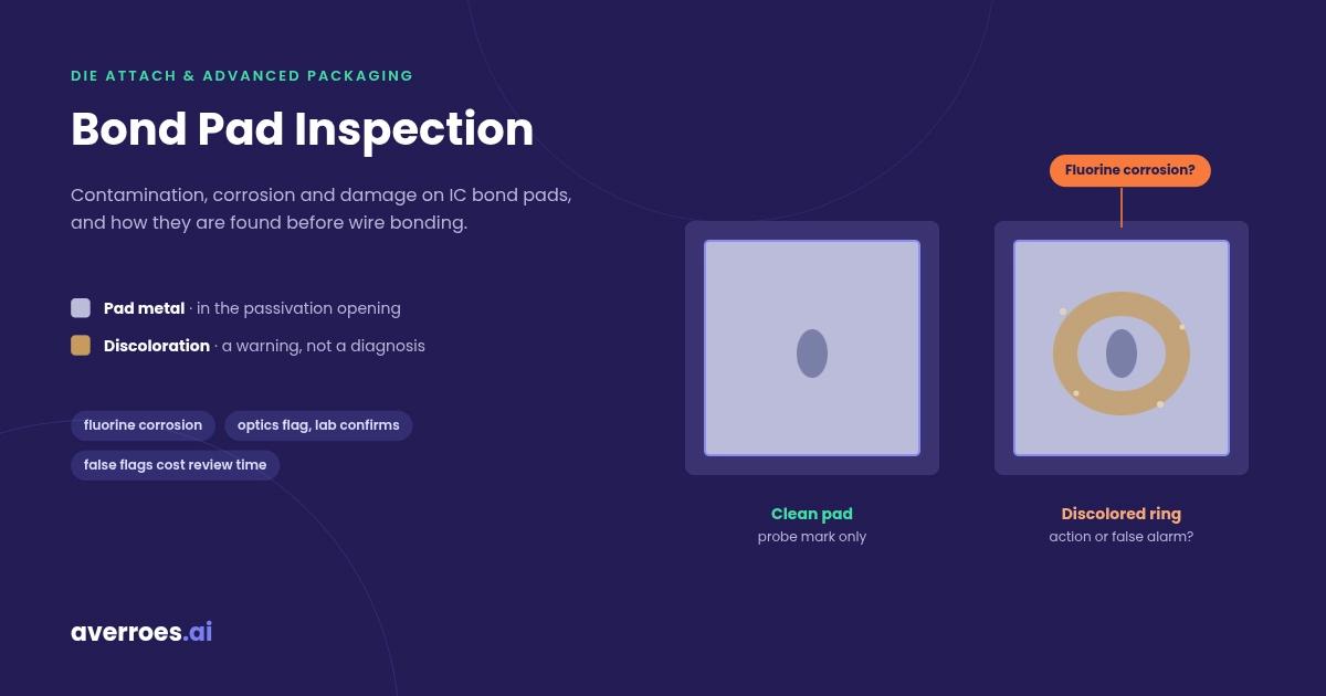
Storage matters too. A 2020 study in the Advances in Science, Technology and Engineering Systems Journal described a donut-shaped discoloration around probe marks, found fluorine only in the discolored ring, identified it as aluminum-fluorine-oxygen corrosion, and pointed to wafer storage as a factor.
The takeaway: the most damaging pad problems are chemical, and they often start before the wafer leaves the fab.
How Are Bond Pads Inspected?
Bond pad inspection is a combination of optical screening, surface analysis and failure analysis, used to find pad problems and confirm their cause before bonding. No single method both screens every pad and identifies the chemistry.
Bond pad inspection methods
Method
What It Sees
Limit
Optical inspection (manual or automated)
Discoloration, residue, scratches, debris, probe marks
Sees color, not chemistry
SEM and EDX
Surface features and rough composition
Lab tool, sampled
Auger electron spectroscopy and XPS
Surface chemistry, including fluorine
Lab tool, sampled, often destructive
GHz acoustic microscopy
Cratering and cracks under the pad
Specialized, sampled
Wire pull and ball shear failure modes
Pad lift or cratering as the failure point
Destructive, after bonding
Optical inspection is the only method that covers every pad at production speed. It runs at wafer back end and at outgoing inspection, where detecting bond pad discoloration is an established task with its own published methods. MIL-STD-883 Method 2010 sets internal visual criteria for high-reliability parts. The lab methods confirm what optics flags: fluorine studies relied on Auger, XPS and similar tools, and an ISTFA 2018 paper showed GHz acoustic microscopy imaging cratering without destroying the part. Imaging and processing methods for die-level optical inspection are covered in die inspection, and dies that pass every screen become known good die.
Is a Discolored Pad Always a Defect?
A pad anomaly is a visible difference from a normal pad, used as a trigger for a decision, not as a verdict. Some anomalies need action: discoloration can be the visible sign of fluorine corrosion that will cause non-sticks. Others do not: a TI failure analysis of a bond pad crack concluded that a minor crack in the pad’s top metal was acceptable, with no impact on electrical performance or reliability for that device.
Inspection systems have long struggled with this. A 2005 Southwest Test Workshop presentation by an inspection equipment maker, August Technology, described probing debris as non-critical to the device yet hard for automated systems to tell apart from defects, making it a source of false defects. In one run without debris filters, the system flagged 7,100 defects that took about 1 hour 10 minutes to review, against 10 minutes 30 seconds of inspection. With an edge debris filter, flags fell to 680 and review to about 7 minutes. The inspection was fast; the review it created was the bottleneck.
The cost of bond pad inspection is in the decision, not the detection: telling a pad that needs action from one that only looks different.
Not Every Pad Anomaly Is a Reject
Test AI defect detection on your own bond pad images
How Is Pad Contamination Removed Before Bonding?
Pad cleaning is a surface treatment that strips contamination and excess oxide from the pad, used just before wire bonding to restore bondability. Plasma and sputter cleaning substantially restore bonding performance after removing fluorine residues and oxide, according to a review of wire bonding pad surface treatments. Sethu’s 2012 review reports that cleaning bond pads with N2/O2 plasma before wire bonding dramatically improved bond strength. Cleaning works best when inspection has flagged which lots need it.
The takeaway: optics screens every pad, the lab confirms the cause, and cleaning or rejection follows.
How Do Bond Pad Defects Cause Wire Bond Failures?
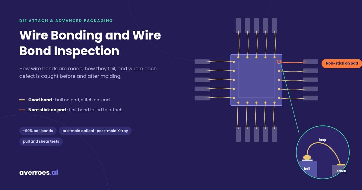
A pad-driven bond failure is a wire bond defect whose root cause is the pad’s condition rather than the bonder, used in failure analysis to point the fix upstream. Contamination, thick oxide and corrosion stop the ball from welding, causing non-stick on pad, or weaken the weld so the ball lifts later.
The link has been shown on real lines. A Peregrine Semiconductor study mapped non-stick on pad back to bond pad contamination and added automated optical inspection at the wafer back end, as covered in wire bonding. Failure analysis follows the same path in reverse: a published failure analysis flow says that once a lifted ball is found, the pad should be inspected for contaminants, deep probe marks or exposed oxide, cratering, metal lifting and corrosion.
Where Does AI Fit in Bond Pad Inspection?
AI bond pad inspection is image-based classification that sorts pad images into specific defect classes and acceptable variation, used to cut false flags without missing pads that need action. The images already exist at wafer back end and outgoing inspection; the problem is deciding what each flag means.
AI does four jobs in bond pad inspection:
Classify pad images into discoloration, corrosion, residue, scratches, debris and probe-related damage.
Separate acceptable variation, such as probing debris that does not affect the device, from defects that need action.
Route suspect pads to failure analysis, so the lab confirms chemistry on the pads most likely to have a problem.
Trend pad defects by wafer, lot and storage time, so a rise in discoloration points to the fab step or storage condition behind it.
Averroes.ai runs AI defect detection and AI defect classification on the optical images a wafer back-end or outgoing inspection line already captures. It trains from 20 to 40 labeled images per defect class, with no code, and deploys on premise. Averroes does not identify chemistry: optical images show the discoloration, and surface analysis confirms its cause. You can test AI defect detection on your own bond pad images.
Frequently Asked Questions
What causes bond pad corrosion?
Bond pad corrosion is most often caused by fluorine left on aluminum pads by the plasma etch that opens them through the passivation. With moisture, the fluorine attacks the aluminum, forming discoloration, aluminum fluoride crystals and thicker oxide. Other contaminants, including chlorine, also contribute, and wafer storage conditions can make it worse.
What does bond pad discoloration mean?
Bond pad discoloration is a visible color change on the pad. It can signal fluorine corrosion, which causes non-stick on pad during wire bonding, but optics alone cannot identify the chemistry. Surface analysis such as Auger or XPS confirms the cause, so discoloration is a reason to investigate, not an automatic reject.
What is bond pad cratering?
Bond pad cratering is damage to the material underneath a bond pad, usually from bonding stress, that can crack the layers below. It is often hidden from optical inspection. It is found by destructive cratering tests, by pull and shear tests that fail at the pad, or non-destructively by GHz acoustic microscopy.
How is bond pad contamination detected?
Bond pad contamination is first flagged by optical inspection, which sees discoloration, stains and residue on every pad. Suspect pads are then analyzed in the lab with SEM and EDX, Auger electron spectroscopy or XPS to identify the contaminant, such as fluorine. Bond failures at the pad also point back to contamination.
How does a contaminated bond pad affect wire bonding?
A contaminated pad stops the wire ball from welding properly. The result is non-stick on pad, where the bond fails to attach, or a weak bond that lifts later. Published studies have traced non-stick on pad to pad contamination, and plasma cleaning before bonding has been shown to restore bond strength.






Bond pad inspection is the check of a die’s bond pads for contamination, corrosion, cracks and damage before wire bonding, because a bad pad causes non-sticks and lifted bonds. Optical inspection finds discoloration, residue and scratches; surface analysis such as Auger or XPS confirms chemistry like fluorine corrosion. AI visual inspection platforms such as Averroes.ai help separate pads that need action from pads that only look different.
Bond pads are probed at wafer test and bonded in Stage 07 of the semiconductor manufacturing process. This guide covers what goes wrong on a pad, how each problem is found, and how to tell a pad that needs action from one that only looks different.
Key Notes
What Is a Bond Pad?
A bond pad is a metal landing area on the top of a die, exposed through an opening in the passivation, used to make electrical contact with the outside world. Most pads are aluminum-based metal over a stack of dielectric and metal layers, with circuitry sometimes running underneath.
A bond pad does two jobs, and both leave their mark. At wafer probe test, probe needles press into the pad to test the die. In assembly, a wire is bonded to the same pad in the die attach and advanced packaging stage. Between the two, the pad has to stay clean, flat and intact enough for wire bonding to form a strong weld.
That makes the pad’s condition a link between two steps owned by different teams. A published review of wire bond visual inspection criteria notes that bond pad inspection before bonding is a critical step that is often overlooked.
What Defects Form on Bond Pads?
A bond pad defect is any contamination, corrosion or physical damage on or under the pad, used as the reason to clean, hold or reject a die before bonding. Some come from the fab, some from probing, and some from storage and handling.
Bond pad defects and how they are found
Probe damage is covered in depth in probe mark inspection. Cracks in the top silicon dioxide film of aluminum pads, from both probing and bonding, are the subject of a 2022 IMAPS paper by onsemi’s Stevan Hunter. The other contaminants come from a review by Sethu in the Australian Journal of Mechanical Engineering (2012), which lists fluorine, chlorine, carbon, oxygen, silicon and titanium among pad contamination sources.
Why Do Aluminum Bond Pads Corrode?
Bond pad corrosion is a chemical attack on the pad metal, most often by fluorine, used in failure analysis as a leading explanation for discolored and non-stick pads. Fluorine contamination on aluminum pads causes corrosion and non-stick on pad, as a 2002 ISTFA study by Hua and colleagues showed, and the corroded areas carried a much thicker aluminum oxide than normal.
The fluorine usually comes from the fab. Residual fluorine on aluminum pads has been traced to the plasma etch that opens the pads through the passivation, which uses hydrofluorocarbon gases. Higher fluorine on the pad surface raises the risk of aluminum fluoride crystals growing, which shows up as discoloration. Moisture makes it worse: an IPC paper by Collier states that residual fluorine on the bond pad leads to corrosion when moisture is present.
Storage matters too. A 2020 study in the Advances in Science, Technology and Engineering Systems Journal described a donut-shaped discoloration around probe marks, found fluorine only in the discolored ring, identified it as aluminum-fluorine-oxygen corrosion, and pointed to wafer storage as a factor.
The takeaway: the most damaging pad problems are chemical, and they often start before the wafer leaves the fab.
How Are Bond Pads Inspected?
Bond pad inspection is a combination of optical screening, surface analysis and failure analysis, used to find pad problems and confirm their cause before bonding. No single method both screens every pad and identifies the chemistry.
Bond pad inspection methods
Optical inspection is the only method that covers every pad at production speed. It runs at wafer back end and at outgoing inspection, where detecting bond pad discoloration is an established task with its own published methods. MIL-STD-883 Method 2010 sets internal visual criteria for high-reliability parts. The lab methods confirm what optics flags: fluorine studies relied on Auger, XPS and similar tools, and an ISTFA 2018 paper showed GHz acoustic microscopy imaging cratering without destroying the part. Imaging and processing methods for die-level optical inspection are covered in die inspection, and dies that pass every screen become known good die.
Is a Discolored Pad Always a Defect?
A pad anomaly is a visible difference from a normal pad, used as a trigger for a decision, not as a verdict. Some anomalies need action: discoloration can be the visible sign of fluorine corrosion that will cause non-sticks. Others do not: a TI failure analysis of a bond pad crack concluded that a minor crack in the pad’s top metal was acceptable, with no impact on electrical performance or reliability for that device.
Inspection systems have long struggled with this. A 2005 Southwest Test Workshop presentation by an inspection equipment maker, August Technology, described probing debris as non-critical to the device yet hard for automated systems to tell apart from defects, making it a source of false defects. In one run without debris filters, the system flagged 7,100 defects that took about 1 hour 10 minutes to review, against 10 minutes 30 seconds of inspection. With an edge debris filter, flags fell to 680 and review to about 7 minutes. The inspection was fast; the review it created was the bottleneck.
The cost of bond pad inspection is in the decision, not the detection: telling a pad that needs action from one that only looks different.
Not Every Pad Anomaly Is a Reject
Test AI defect detection on your own bond pad images
How Is Pad Contamination Removed Before Bonding?
Pad cleaning is a surface treatment that strips contamination and excess oxide from the pad, used just before wire bonding to restore bondability. Plasma and sputter cleaning substantially restore bonding performance after removing fluorine residues and oxide, according to a review of wire bonding pad surface treatments. Sethu’s 2012 review reports that cleaning bond pads with N2/O2 plasma before wire bonding dramatically improved bond strength. Cleaning works best when inspection has flagged which lots need it.
The takeaway: optics screens every pad, the lab confirms the cause, and cleaning or rejection follows.
How Do Bond Pad Defects Cause Wire Bond Failures?
A pad-driven bond failure is a wire bond defect whose root cause is the pad’s condition rather than the bonder, used in failure analysis to point the fix upstream. Contamination, thick oxide and corrosion stop the ball from welding, causing non-stick on pad, or weaken the weld so the ball lifts later.
The link has been shown on real lines. A Peregrine Semiconductor study mapped non-stick on pad back to bond pad contamination and added automated optical inspection at the wafer back end, as covered in wire bonding. Failure analysis follows the same path in reverse: a published failure analysis flow says that once a lifted ball is found, the pad should be inspected for contaminants, deep probe marks or exposed oxide, cratering, metal lifting and corrosion.
Where Does AI Fit in Bond Pad Inspection?
AI bond pad inspection is image-based classification that sorts pad images into specific defect classes and acceptable variation, used to cut false flags without missing pads that need action. The images already exist at wafer back end and outgoing inspection; the problem is deciding what each flag means.
AI does four jobs in bond pad inspection:
Averroes.ai runs AI defect detection and AI defect classification on the optical images a wafer back-end or outgoing inspection line already captures. It trains from 20 to 40 labeled images per defect class, with no code, and deploys on premise. Averroes does not identify chemistry: optical images show the discoloration, and surface analysis confirms its cause. You can test AI defect detection on your own bond pad images.
Frequently Asked Questions
What causes bond pad corrosion?
Bond pad corrosion is most often caused by fluorine left on aluminum pads by the plasma etch that opens them through the passivation. With moisture, the fluorine attacks the aluminum, forming discoloration, aluminum fluoride crystals and thicker oxide. Other contaminants, including chlorine, also contribute, and wafer storage conditions can make it worse.
What does bond pad discoloration mean?
Bond pad discoloration is a visible color change on the pad. It can signal fluorine corrosion, which causes non-stick on pad during wire bonding, but optics alone cannot identify the chemistry. Surface analysis such as Auger or XPS confirms the cause, so discoloration is a reason to investigate, not an automatic reject.
What is bond pad cratering?
Bond pad cratering is damage to the material underneath a bond pad, usually from bonding stress, that can crack the layers below. It is often hidden from optical inspection. It is found by destructive cratering tests, by pull and shear tests that fail at the pad, or non-destructively by GHz acoustic microscopy.
How is bond pad contamination detected?
Bond pad contamination is first flagged by optical inspection, which sees discoloration, stains and residue on every pad. Suspect pads are then analyzed in the lab with SEM and EDX, Auger electron spectroscopy or XPS to identify the contaminant, such as fluorine. Bond failures at the pad also point back to contamination.
How does a contaminated bond pad affect wire bonding?
A contaminated pad stops the wire ball from welding properly. The result is non-stick on pad, where the bond fails to attach, or a weak bond that lifts later. Published studies have traced non-stick on pad to pad contamination, and plasma cleaning before bonding has been shown to restore bond strength.