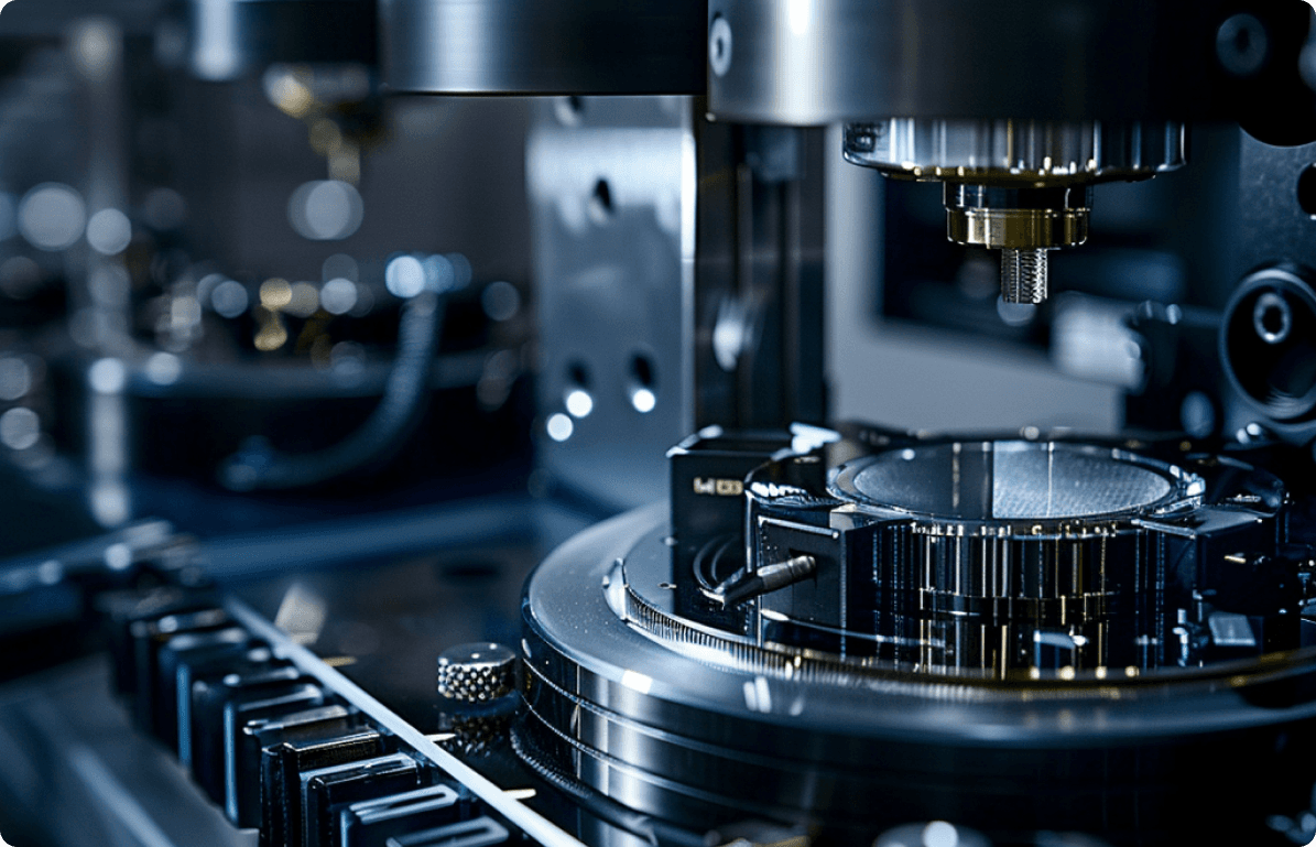
Film Thickness Measurement with Deep Learning
in Semiconductor Manufacturing
Our advanced AI ensures precise film application and superior uniformity across all dies - crucial for consistent device performance.
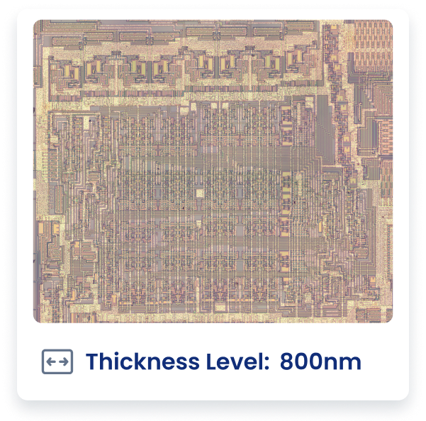
Image-Based Metrology Enhancements
Our virtual metrology system analyzes images captured during film deposition, providing high-precision assessments of film thickness and uniformity. Detect even subtle variations invisible to traditional methods.
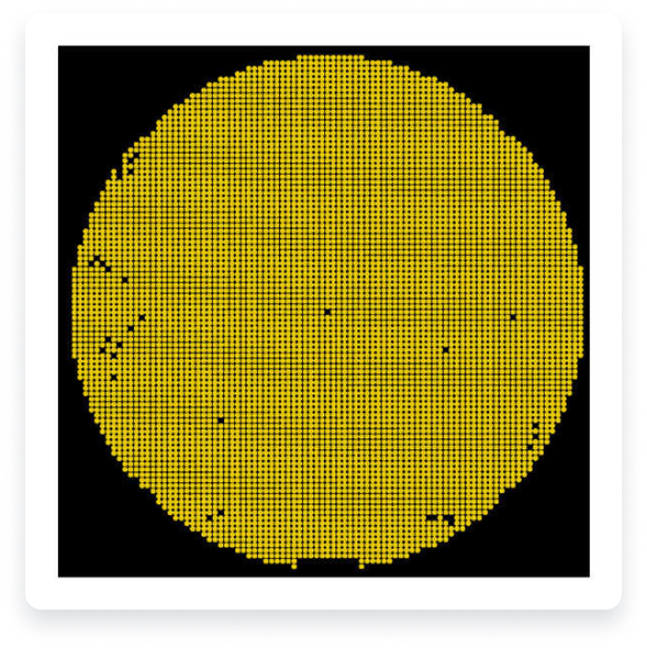
Automated Die Distribution Analysis
Analyze film thickness distribution across individual dies to ensure uniform material deposition. Maintain consistent device performance across the entire wafer with our automated die distribution analysis.
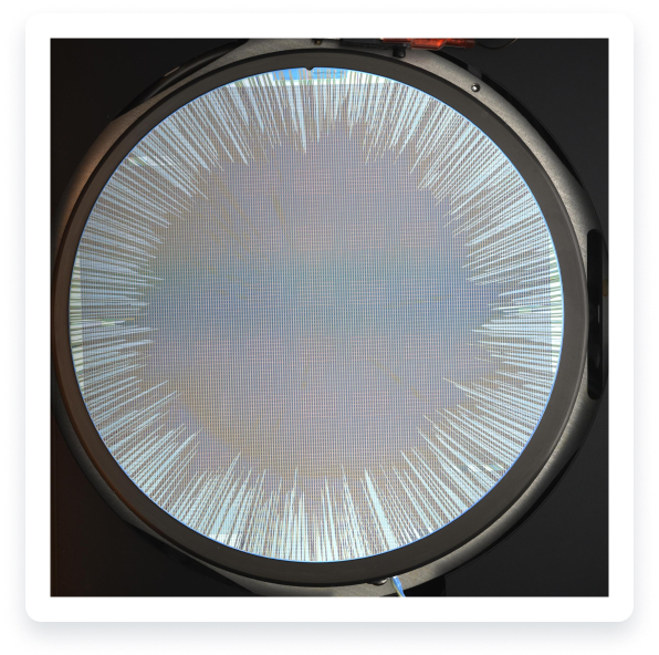
Real-Time Thickness Monitoring
Our deep learning virtual metrology system processes metrology data in real time, providing immediate feedback to deposition equipment. This enables dynamic adjustments to the film application process, ensuring optimal film uniformity and correcting any detected anomalies or deviations.
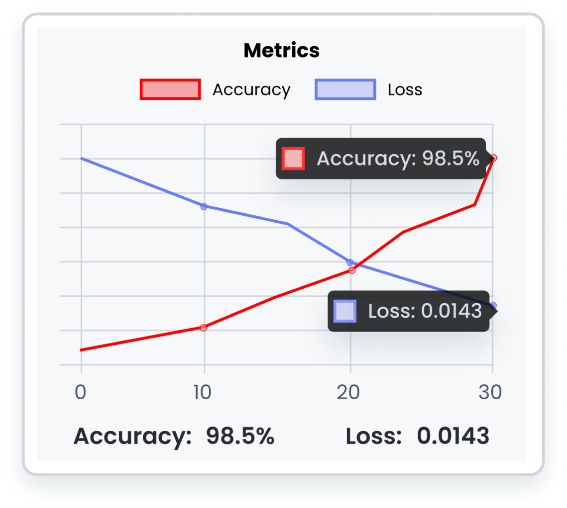
Continuously Learns From Data
Unlike traditional systems, our model continuously learns from data, improving accuracy and performance over time. This ensures consistent high performance and delivers evolving accuracy via Averroes' Active Learning feature.
Privacy and Security
Choose on-premise for privacy, speed, and security or cloud for scalability and performance. We're cloud-agnostic, ensuring seamless integration and flexibility.
We've experienced a remarkable 40-60% increase in submicron defect detection. Averroes has saved us over 300 hours/month/app of labor and increased our productivity by more than 30% .
Automation Manager @ Semiconductor OEM
Frequently asked questions
Our deep learning virtual metrology uses advanced algorithms to analyze images, detecting subtle variations missed by traditional methods. This results in significantly improved precision and uniformity.
Experience the Averroes AI Advantage
Elevate Your Visual Inspection Capabilities
Request a Demo Now
