Semiconductor Manufacturing Process: All 12 Stages From Silicon Ingot to Finished Chip
What happens at each stage, which defects originate there, how the stage is inspected today, and where AI inspection changes the outcome.
Semiconductor manufacturing turns a cylinder of ultra-pure silicon into packaged, tested chips across 12 stages. The process runs from crystal growth and wafer preparation, through hundreds of front-end fabrication cycles that build transistor structures layer by layer, then through probe test, dicing, packaging, final test, marking and packing before shipment to OEMs.
Eight of those 12 stages have a visual inspection gate. A defect that passes one of them costs roughly ten times more to catch at the next.
- An advanced logic node runs over 1,000 process steps across 50 to 100 mask layers, all inside Stage 3 alone.
- Defects rarely surface where they are created. Crystal defects from Stage 1 print through at Stage 3 and fail electrically at Stage 5.
- False positives cost as much as escapes. Over-rejection scraps yield, and it pushes operators to loosen thresholds.
- Coverage at eight gates costs less than escape at one.
The 12 stages at a glance
Semiconductor manufacturing turns a cylinder of ultra-pure silicon into packaged, tested chips across 12 stages. Eight of them carry a visual inspection gate — and a defect that passes one costs roughly ten times more to catch at the next.
| # | Stage | What happens | Primary defect class | Inspection method | VI gate |
|---|---|---|---|---|---|
| 01 | Silicon Ingot | Czochralski crystal growth | Dislocations, oxygen precipitates | Resistivity, X-ray topography | No |
| 02 | Wafer Manufacturing | Slice, lap, etch, polish | Saw marks, TTV, edge chips | Surface scan, flatness metrology | No |
| 03 | Wafer Fabrication | Litho, etch, deposition, CMP | Particles, bridges, opens, residue | Brightfield, darkfield, e-beam | Yes |
| 04 | Inspection & Metrology | Defect scan, CD, overlay, film | Pattern defects, CD drift | Optical, SEM, scatterometry | Yes |
| 05 | Wafer Probe | On-wafer electrical test | Probe marks, pad damage | Probe mark inspection, wafer map | Yes |
| 06 | Wafer Dicing | Blade, laser or plasma singulation | Chipping, cracks, delamination | Post-dicing optical inspection | Yes |
| 07 | Die Attach & Packaging | Die mount, wire bond, flip chip | Bond lifts, voids, coplanarity | Optical AOI, X-ray, CT | Yes |
| 08 | Final Test & Burn-In | Electrical retest under stress | Cracks, delamination, popcorning | Post burn-in visual screening | Yes |
| 09 | Marking & Inspection | Laser mark, cosmetic gate | Illegible marks, chips, scratches | OCR/OCV, cosmetic AOI | Yes |
| 10 | Tape & Reel | Load into carrier for SMT | Wrong orientation, empty pockets | Inline carrier inspection | Partial |
| 11 | Shipping to OEMs | Dry pack, label, distribute | Counterfeits, MSL breaches | Incoming authentication | No |
| 12 | Final Products | SMT assembly onto PCB | Solder defects, voids | AOI, AXI at OEM | No |
Where Defects Enter and Where They Escape
Defects do not distribute evenly across the process. They originate at specific steps, and they surface at very different points from where they were created. Three things make this expensive.
Cost compounds downstream
The rule of ten holds across the whole lifecycle. A particle found at post-develop inspection costs a rework cycle. The same particle found at final test has consumed the full fabrication, dicing, packaging and test cost of that die. Found in the field, it costs a recall.
Detection lags creation
Crystal-origin defects from Stage 1 do not become visible until they print through in Stage 3 or fail electrically in Stage 5. Package voids introduced in Stage 7 often survive final test and fail after thermal cycling. This is why inspection at a single gate does not work. Coverage has to be distributed.
False positives cost as much as escapes
Every over-rejected die is scrapped yield. Every over-called defect pulls an engineer into manual review. Fabs running rule-based inspection routinely see nuisance rates high enough that operators raise thresholds, which is precisely how escapes happen.
Defect origin versus detection point
| Originates at | Defect | Typical size | Usually detected at |
|---|---|---|---|
| Stage 1 | Crystal dislocations, slip | Sub-micron | Stage 3 or 5 |
| Stage 2 | Edge chips, TTV, saw damage | 10 to 500 µm | Stage 2 or 3 |
| Stage 3 | Particles, bridging, opens | 20 nm to 10 µm | Stage 3 or 4 |
| Stage 3 | Post-CMP scratches, dishing, residue | 0.1 to 50 µm | Stage 4 |
| Stage 5 | Probe mark damage, pad cratering | 5 to 50 µm | Stage 5 or 8 |
| Stage 6 | Chipping, backside cracks | 5 to 200 µm | Stage 6 or 8 |
| Stage 7 | Bond lifts, voids, bump coplanarity | 1 to 100 µm | Stage 7 or field |
| Stage 9 | Cosmetic damage, mark defects | 20 µm and up | Stage 9 or 12 |
For the inspection methods themselves rather than the process steps, start with semiconductor inspection and metrology explained.
Silicon Ingot Growth
Ultra-pure polysilicon is melted and pulled into a single-crystal cylindrical ingot using the Czochralski process. A 300 mm ingot runs roughly 2 metres long and weighs several hundred kilograms.
What happens at this stage
Electronic-grade polysilicon is charged into a quartz crucible and heated past 1,414 °C. Dopant is added to set the target resistivity. A seed crystal is lowered to the melt surface, then withdrawn while both seed and crucible counter-rotate. Pull rate and thermal gradient control the diameter and the defect density of the growing crystal.
Float-zone growth is the alternative route for very high resistivity applications, mainly power devices and detectors. Czochralski dominates by volume because it scales to 300 mm economically. The ingot is then cropped, ground to diameter, and marked with a notch that fixes crystal orientation for every downstream tool.

Defects that originate here5
- Dislocations and slip lines from thermal shock during seeding or pulling
- Oxygen precipitates from crucible dissolution, which nucleate stacking faults later
- COPs, vacancy clusters that behave like sub-surface voids
- Resistivity variation radially and axially along the ingot
- Carbon and metallic contamination from the crucible and hot zone
None of these are visible defects at this stage. They are latent, and they surface as yield loss 200 process steps later.
How this stage is inspected
Resistivity is mapped with four-point probe. Oxygen and carbon content are measured by FTIR. Minority carrier lifetime testing screens for metallic contamination. X-ray topography and preferential etching reveal dislocation structure on sample slices. Inspection here is destructive and sample-based, not inline and not visual.
Deep dives3
- What is the Czochralski Process? — coming
- Silicon Ingot Defects and Downstream Yield — coming
- Monocrystalline vs Polycrystalline Silicon — coming
Crystal quality sets the floor on everything downstream. A wafer with high COP density will generate gate oxide failures no amount of process control can recover.
Wafer Manufacturing
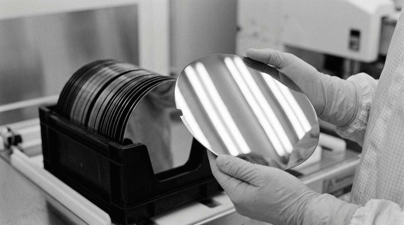
The ingot is sliced into thin wafers and processed to a mirror finish. A finished 300 mm wafer is roughly 775 µm thick with total thickness variation under 1 µm and surface roughness measured in angstroms.
What happens at this stage
Slicing is done with a diamond wire saw, which leaves subsurface damage several microns deep. Lapping and grinding remove that damage layer and bring the wafer into flatness spec. Chemical etching removes the remaining mechanical damage. Edge profiling rounds the wafer rim so it resists chipping and particle generation in later handling.
CMP produces the final device-side surface. The wafer is then cleaned through an RCA sequence, dried, and inspected before packing in a FOUP. Key specifications set here: diameter, thickness, TTV, bow and warp, site flatness, edge exclusion, resistivity, crystal orientation and particle count.
Defects that originate here5
- Saw marks and subsurface damage left by incomplete lapping
- Edge chips and cracks that propagate inward under thermal stress
- Bow and warp exceeding lithography chuck tolerance
- Particles and haze from incomplete cleaning
- Backside contamination that causes focus errors at lithography
How this stage is inspected
Laser surface scanners count and size particles across the full wafer at incoming inspection. Capacitive or optical flatness tools measure TTV, bow, warp and site flatness. Haze measurement quantifies surface roughness. Edge inspection systems image the bevel and apex.
Backside condition matters more than most incoming specs suggest, because backside particles translate directly into front-side overlay and focus error. See backside wafer inspection for the tooling and failure modes, and wafer bow and warp measurement for how substrate geometry propagates into yield.
Deep dives4
- How Silicon Wafers Are Made — coming
- Silicon Wafer Specifications Explained — coming
- Top Silicon Wafer Manufacturers 2026 — coming
- Wafer Polishing and Surface Preparation — coming
Substrate quality defines the detection floor for everything after it. If incoming wafers carry a variable particle baseline, every inline inspection at Stage 3 inherits that noise.
Wafer Fabrication (Front-End)
Transistor structures are built layer by layer through repeated cycles of deposition, lithography, etch, implant and planarisation. This is where most defects are created.
What happens at this stage
Each layer follows the same loop. Deposition lays down oxide, nitride, polysilicon or metal by CVD, PVD or ALD. Photoresist coat applies a light-sensitive film on a track. Lithography projects the mask pattern through a stepper or scanner, at advanced nodes using EUV at 13.5 nm wavelength. Develop removes exposed or unexposed resist. Etch transfers that pattern into the underlying film. Strip and clean removes remaining resist. Ion implantation dopes exposed silicon. CMP planarises the surface so the next layer prints in focus.
For the patterning step in detail, see the photolithography process. For the mask itself, see photomask inspection and reticle inspection, since a single reticle defect repeats across every die on every wafer exposed with it.

Defects that originate here6
- Particles from tools, chemistry and handling, killer size scales with node
- Pattern bridging and opens from resist, focus or etch excursions
- Post-CMP scratches, dishing and erosion, plus slurry residue
- Voids and stringers in metal layers
- Edge and bevel defects that flake and redeposit on the device area
- Overlay and CD excursions that print correctly but measure out of spec
How this stage is inspected
Inline inspection runs after the highest-risk steps rather than after every step. Common gates are post-develop, post-etch, post-CMP and post-metal deposition.
Brightfield inspection collects specularly reflected light and finds pattern defects on planar surfaces. Darkfield inspection collects scattered light and is more sensitive to particles and to defects on rough topography. Macro inspection covers full-wafer signatures like coating streaks and handling damage. E-beam inspection trades throughput for resolution and catches voltage contrast defects optical tools cannot see.
For the full front-end methodology, sensitivity trade-offs and sampling strategy, see the front-end wafer inspection hub. For defect types by surface rather than by step, see surface defect inspection.
Deep dives8
- Photoresist Coat Inspection — coming
- Post-Etch Inspection — coming
- Post-CMP Inspection — coming
- Thin Film and Metal Layer Inspection — coming
- Post-Develop Inspection (PDI) — coming
- Overlay Metrology — coming
- Wafer Edge and Bevel Inspection — coming
- Particle Contamination Inspection — coming
Full sensitivity without the nuisance rate
Front-end inspection fails in one of two directions: sensitivity low enough to keep nuisance rates workable, which lets real defects through, or sensitivity high enough to catch everything, which buries review engineers. Averroes AI trains on 20 to 40 images per defect class and runs as an overlay on the inspection tools already installed. Customers hold near zero false positives at full sensitivity. No hardware replacement, no code.
Wafer Inspection and Metrology
Defect inspection finds what should not be there. Metrology measures whether what should be there is correct. Both run between process steps, and together they feed the control loops that keep the line in spec.
What happens at this stage
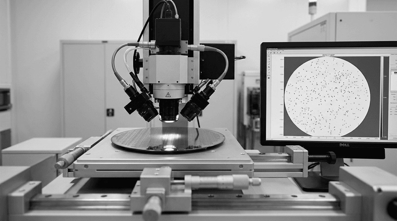
Defect inspection scans the wafer for anomalies and produces a defect map with coordinates, size and classification. Comparison is die-to-die on production wafers, or die-to-database against the intended layout when neighbouring dies cannot be trusted as reference.
Metrology measures dimensions and material properties. CD measurement by CD-SEM or scatterometry confirms feature width. Overlay metrology confirms layer-to-layer alignment. Ellipsometry and reflectometry confirm film thickness. See metrology tools, how defect metrology works and the wafer inspection guide.
How inspection output becomes process control3 loops
- Classification. Manual defect review does not scale to modern defect counts. See automatic defect classification and wafer defect detection.
- Fault detection and process control. Sensor and metrology data feed systems that flag tool excursions before they print. See FDC systems and advanced process control.
- Prediction. Virtual metrology predicts measurement values from process data instead of measuring every wafer, raising effective sampling without adding metrology capacity.
Root cause work and the data layer underneath both sit here: automated root cause analysis and defect data management.
Deep dives4
- Pattern Defect Inspection — coming
- Wafer Defect Map Analysis — coming
- Applied Materials Tools Review — coming
- Wafer Notch Inspection — coming
Review without the manual queue, metrology without new tools
Automated judgment classifies and dispositions flagged sites at production volume with near zero false positives, so review headcount stops being the throughput limit. Virtual metrology predicts parameters from data the fab already collects, feeding the APC loop with full-lot coverage rather than sampled coverage.
Wafer Probe and Electrical Test
Every die is electrically tested while still on the wafer. Only dies that pass go forward, because packaging a bad die wastes the entire packaging and test cost attached to it.
What happens at this stage
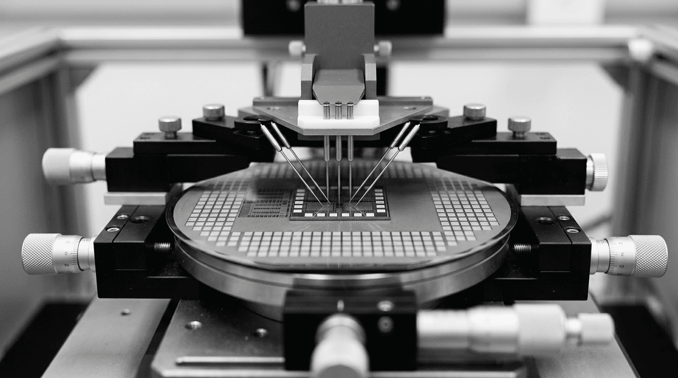
A probe card lands fine needles or vertical probes on the die bond pads. Automated test equipment runs functional, parametric and sometimes at-speed patterns. Results are binned, and the prober builds a wafer map. Modern lines use inkless mapping, where the map travels electronically rather than as an ink dot on failed dies. Probing is mechanically aggressive by design, because the probe has to break through pad oxide to make contact.
Defects that originate or surface here4
- Probe mark damage: excessive depth, off-centre landing, pad cratering
- Pad contamination transferred from probe tips
- Electrical failures that trace back to Stage 1 crystal defects or Stage 3 pattern defects
- Systematic spatial fail patterns: edge rings, radial gradients, cluster signatures
How this stage is inspected
Probe mark inspection images pads post-probe to confirm mark size, depth and placement are within spec. The wafer map itself is the second inspection output, and its spatial pattern is diagnostic. Edge failures point to one set of causes, centre clusters to another.
The high-value work here is correlation. A visual defect map from Stage 4 and an electrical bin map from Stage 5 describe the same wafer. Overlaying them shows which visual defect classes actually kill dies. See defect data management for the infrastructure that makes it possible.
Deep dives2
- Wafer Probe Visual-Electrical Correlation — coming
- Die Sorting and Inkless Map Verification — coming
Visual and electrical data on the same wafer map
The two data streams usually live in separate systems and get compared manually, if at all. Averroes AI monitors both and surfaces the correlation, so die sorting decisions use visual evidence alongside electrical results rather than after them.
Wafer Dicing
The tested wafer is singulated into individual dies by blade sawing, laser dicing or plasma dicing. Each method produces a different edge quality and a different defect signature.
What happens at this stage
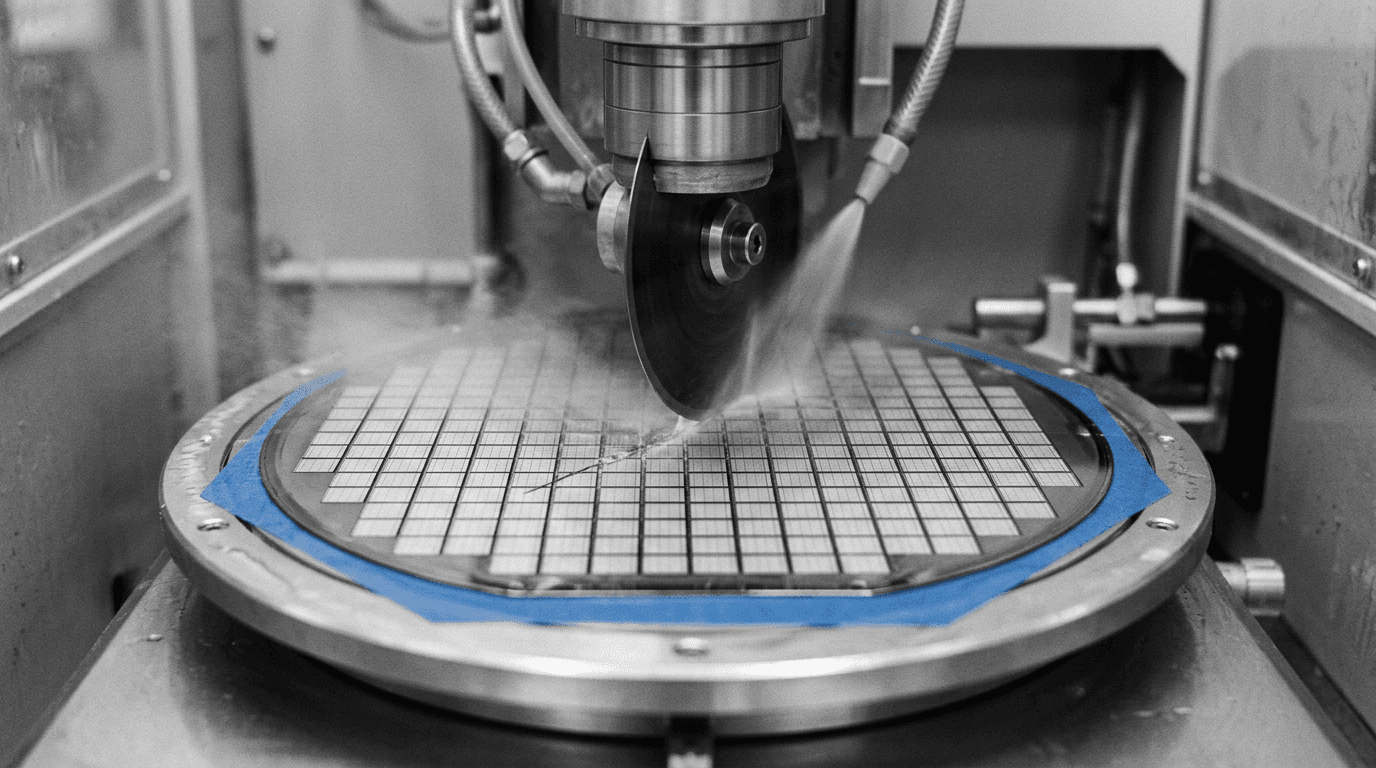
The wafer is mounted on dicing tape on a frame. Blade dicing cuts a kerf with a resin-bonded diamond blade. Laser dicing ablates or, in stealth dicing, focuses below the surface to create a modified layer that separates when the tape is expanded. Plasma dicing etches the streets chemically, which gives the cleanest edge and suits very thin or non-rectangular dies.
Die thickness at advanced packaging can drop below 50 µm, which makes edge quality a first-order reliability concern rather than a cosmetic one.
Defects that originate here5
- Chipping on front side and back side along the cut edge
- Cracks propagating from the kerf into the active area
- Delamination of film stacks at the die edge
- Kerf deviation and street misalignment
- Burr, debris and tape residue on the die surface or backside
A die edge crack that clears visual inspection frequently survives final test and fails after thermal cycling in the field. This is the classic latent defect of the back end.
How this stage is inspected
Post-dicing optical inspection images each die at production speed, front and back, looking at the edge specifically rather than the active area. Confocal and laser scanning methods measure chip depth. See crack detection and inspection for methods and failure modes.
The difficulty is discrimination. Blade and laser dicing both leave normal artefacts along every edge. Distinguishing an acceptable process signature from a genuine chip out of spec is a classification problem, not a threshold problem.
Deep dives2
- Post-Dicing Die Edge Inspection — coming
- Wafer Dicing Quality and Singulation — coming
Learns your dicing signature, not a generic threshold
Trained on the line's own images, the model learns what a normal edge looks like for that blade, that material and that recipe, then flags genuine excursions. Near zero false positives means the line stops scrapping good dies for cosmetic kerf variation.
Die Attach and Advanced Packaging
Known-good dies are mounted into a package and connected to the outside world. This stage carries the highest defect variety in the lifecycle, because it combines materials, mechanics, thermal processes and fine-pitch interconnect in one flow.
What happens at this stage
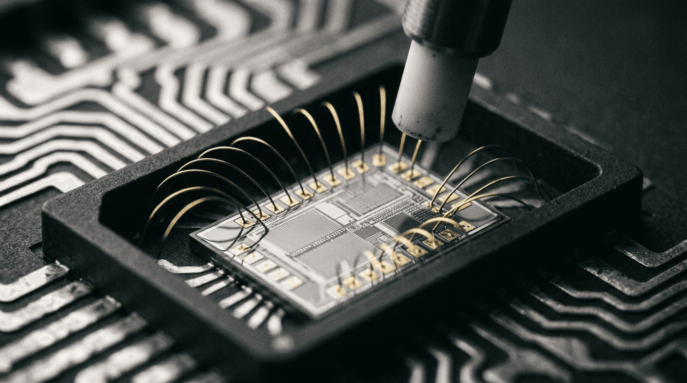
Die attach bonds the die to a leadframe, substrate or another die using epoxy, film adhesive or eutectic solder. Interconnect is either wire bonding or flip chip, where the die is inverted onto solder bumps or copper pillars and reflowed. Underfill flows beneath flip-chip dies to manage thermal stress. Encapsulation moulds the package. Ball attach places the solder balls for BGA packages.
Advanced packaging adds interposers, through-silicon vias, redistribution layers and stacked die. See metrology innovations for advanced packaging for the measurement challenges introduced by stacking.
Defects that originate here7
- Die attach voids, tilt and bleed-out
- Wire bond failures: non-stick on pad, lifted ball, sagging loop, wire sweep, shorts
- Bond pad damage and oxidation preventing reliable bonding
- Solder bump defects: missing bumps, bridging, coplanarity variation, head-in-pillow
- Underfill voids and incomplete flow
- Mould defects: incomplete fill, flash, delamination at interfaces
- BGA ball defects: missing, misaligned, voided or non-wetted balls
How this stage is inspected
Optical AOI handles anything visible from above: wire loop profile, ball placement, package cosmetics, marking. See PCB and component visual inspection for the shared method set.
X-ray is mandatory for anything hidden. Solder joints under a BGA, bumps under a flip-chip die, die attach voids and wire sweep inside a moulded package are all invisible to optical methods. See automated X-ray inspection systems.
The inspection problem here is surface variety. Reflective solder, matte mould compound, fine gold wire and textured substrate all appear in the same field of view, and each requires different imaging treatment.
Deep dives6
- Wire Bond Inspection — coming
- Bond Pad Inspection — coming
- Flip-Chip and Solder Bump Inspection — coming
- BGA Inspection — coming
- IC Package Cosmetic Inspection — coming
- Data Annotation for Defect Models — coming
New package types onboarded in days, not quarters
Packaging lines change constantly: new package types, new pitches, new ball counts, new substrate suppliers. Rule-based AOI recipes have to be rebuilt each time. Averroes AI learns each configuration from 20 to 40 labelled images per defect class and keeps learning from operator dispositions in production.
Final Test and Burn-In
The packaged device is retested electrically through its finished package, then stressed to force early-life failures to occur before shipment rather than in the field.
What happens at this stage
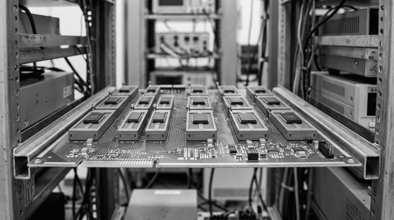
Final test runs the device on ATE through functional, parametric and speed-sorting patterns across the full temperature range. Devices are binned by speed grade and quality level. Burn-in applies elevated temperature and voltage for hours to accelerate infant mortality failures, the early part of the bathtub curve. Automotive and high-reliability parts get extended burn-in. See semiconductor reliability testing for the qualification framework behind these decisions.
Defects that surface here5
- Package cracking from thermal cycling stress
- Popcorning: absorbed moisture vaporising and delaminating the package
- Solder ball fatigue and cracking after thermal stress
- Substrate warpage exceeding coplanarity spec
- Latent Stage 6 and 7 defects finally propagating to failure
How this stage is inspected
Electrical test does the primary screening. Visual inspection after burn-in is the underused gate. Parts come out of burn-in physically stressed, and defects that were sub-critical before are now visible: hairline package cracks, delamination fringes, ball deformation, socket damage on the leads. Acoustic microscopy detects internal delamination non-destructively.
Deep dives1
- Post Burn-In Visual Inspection — coming
Post-stress screening at line speed
Post burn-in visual screening is often skipped because it adds a manual step at the end of a long flow. Automated screening runs it at line speed with continuous monitoring across lots, so drift in post-stress defect rates becomes an early signal on the packaging process rather than a field return six months later.
Marking and Final Visual Inspection
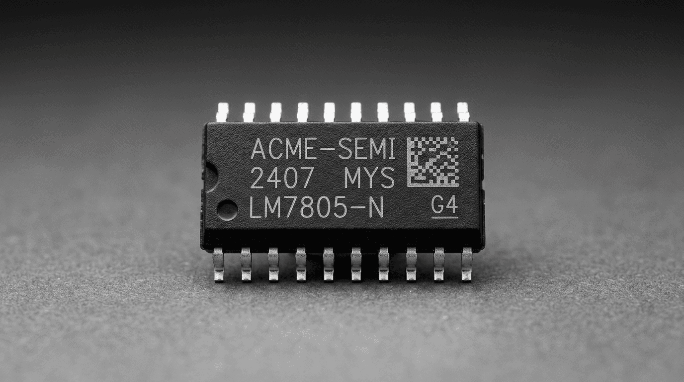
Every device is laser marked with part number, lot code, date code and often a 2D data matrix. It then passes the final cosmetic gate — the last point at which the manufacturer sees the part before the customer does.
What happens at this stage
Laser marking ablates or discolours the package surface. The mark carries traceability data linking the finished device back to its wafer, lot and fab. Final visual inspection checks two things at once: that the mark is correct and legible, and that the package itself is cosmetically and dimensionally acceptable. Lead coplanarity, pin count, package dimensions and orientation are verified in the same pass on most lines.
Defects caught here4
- Mark defects: illegible characters, wrong content, offset placement, low contrast
- Package cosmetics: chips, scratches, dents, flash, contamination, discolouration
- Lead and ball defects: bent leads, coplanarity out of spec, missing balls
- Mixed lots: wrong device in the wrong carrier
How this stage is inspected
OCR and OCV read the mark and verify it against expected content. Data matrix codes are read and validated. Cosmetic inspection runs AOI against a golden reference. See automated visual inspection systems explained, label inspection and vision systems for final product quality.
Cosmetic inspection is where false rejects concentrate. Package surfaces vary batch to batch in texture and colour, lighting shifts, and threshold-based systems respond by over-rejecting. Operators then loosen thresholds, and escapes follow.
Deep dives2
- Laser Mark and Traceability Inspection — coming
- Tray and Carrier Inspection — coming
Holds calibration across mould compound batches
The model learns the acceptable appearance range for that package type from the line's own images, rather than being tuned against a single golden sample. OCR runs at line speed with near zero false rejects, and active learning absorbs operator dispositions so the model tracks the line instead of drifting from it.
Tape and Reel and Tray Packaging
Finished devices are loaded into carriers designed for automated pick-and-place at the customer's SMT line. Tape and reel dominates for high-volume parts, JEDEC trays for larger packages.
What happens at this stage
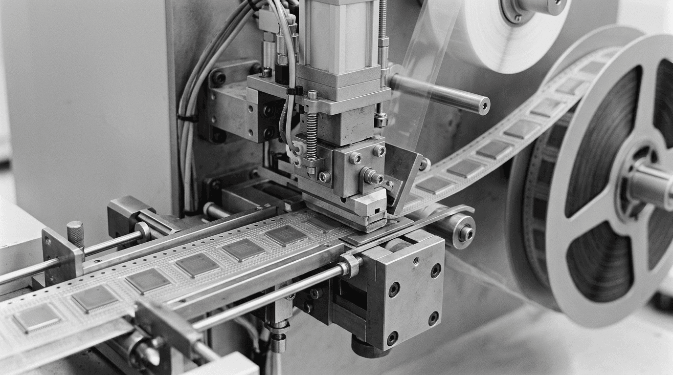
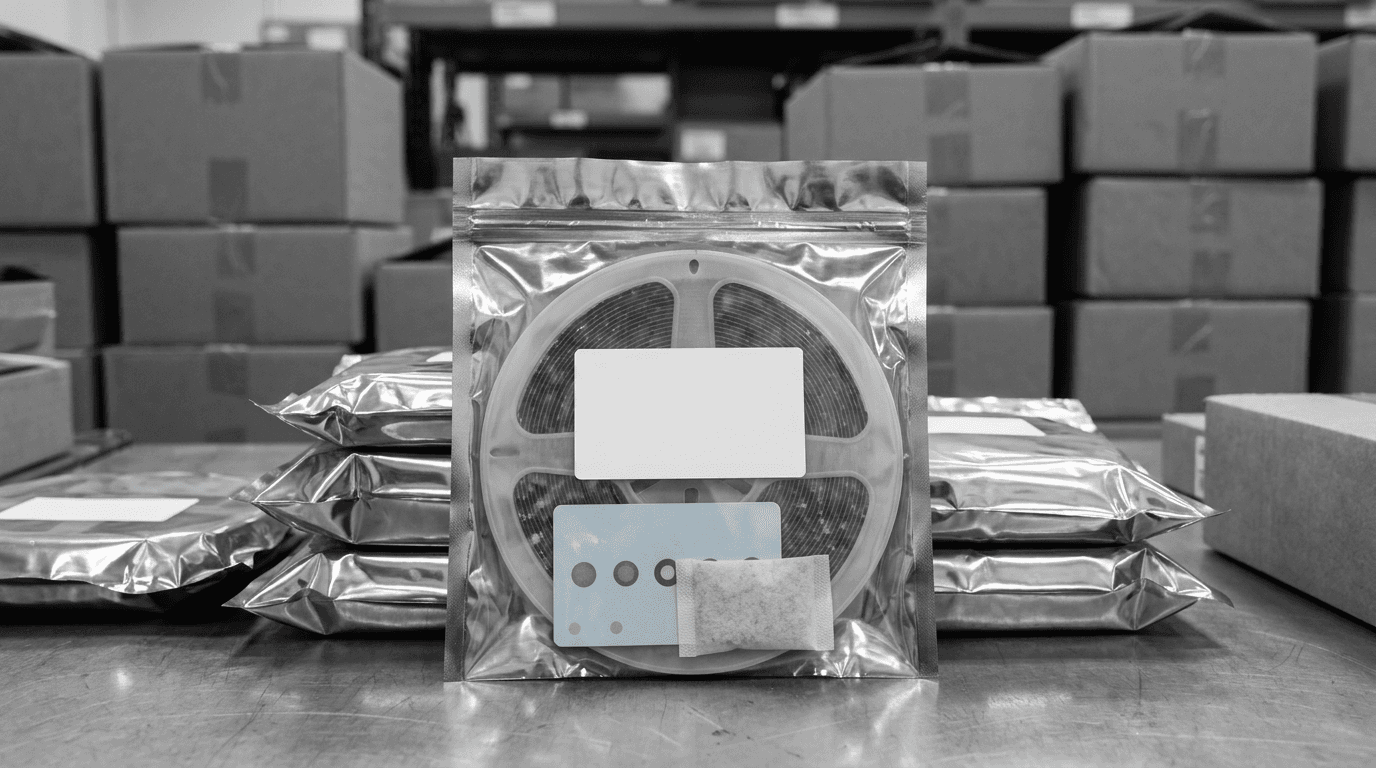
Devices are placed into embossed pockets in carrier tape, sealed under cover tape, and wound onto reels. Pocket pitch, tape width and reel dimensions follow EIA-481. Trays follow JEDEC outlines. Moisture-sensitive devices are vacuum sealed in a barrier bag with desiccant and a humidity indicator card, labelled with the applicable MSL rating.
Defects caught here5
- Empty pockets in a sealed reel
- Wrong orientation: parts rotated 90 or 180 degrees relative to pin 1
- Damage during placement: bent leads, scratched surfaces
- Cover tape defects: poor seal, peel force out of spec, wrinkles
- Mixed devices or label mismatch between carrier contents and outer label
An orientation error found at the customer's SMT line stops their production. It is a small defect with a large commercial consequence.
How this stage is inspected
Inline vision checks presence, orientation and polarity as devices enter each pocket, before the cover tape seals. Post-seal inspection verifies seal integrity and can count parts optically through clear cover tape. The same visual inspection quality control principles apply, at carrier scale rather than device scale.
Deep dives3
- Tape and Reel Inspection — coming
- IC Tray Packaging Standards — coming
- EIA-481 Standards Guide — coming
Shipping to OEMs
Packed devices move through distribution to OEMs, contract manufacturers and board assemblers. The manufacturing process is finished, but the quality chain is not.
What happens at this stage
Reels and trays are boxed, labelled with part number, lot code, quantity and MSL rating, and shipped either direct to the OEM or through authorised distribution. Moisture-sensitive parts carry a floor life clock that starts when the barrier bag is opened. Traceability data assembled across all previous stages travels with the lot, and it is what makes a field failure traceable back to a fab, a lot and in some cases a specific wafer.
Risks at this stage4
- Counterfeit and recycled parts entering through unauthorised distribution
- Remarked devices: lower-grade parts relabelled as higher-grade
- MSL breaches from bags opened and resealed without a bake cycle
- Mislabelled or mixed lots, ESD and mechanical damage in transit
How this is controlled
Authentication combines external visual inspection, mark verification, X-ray comparison against a known-good reference, decapsulation on samples and electrical verification. The visual layer catches most of it, because remarking leaves evidence: surface texture inconsistent with factory laser marking, sanding marks, resurfacing compound, mark content that does not match the die inside. See automatic defect classification.
Deep dives3
- Semiconductor Traceability — coming
- Counterfeit Semiconductor Detection — coming
- Supply Chain Quality Standards — coming
Integration into Final Products
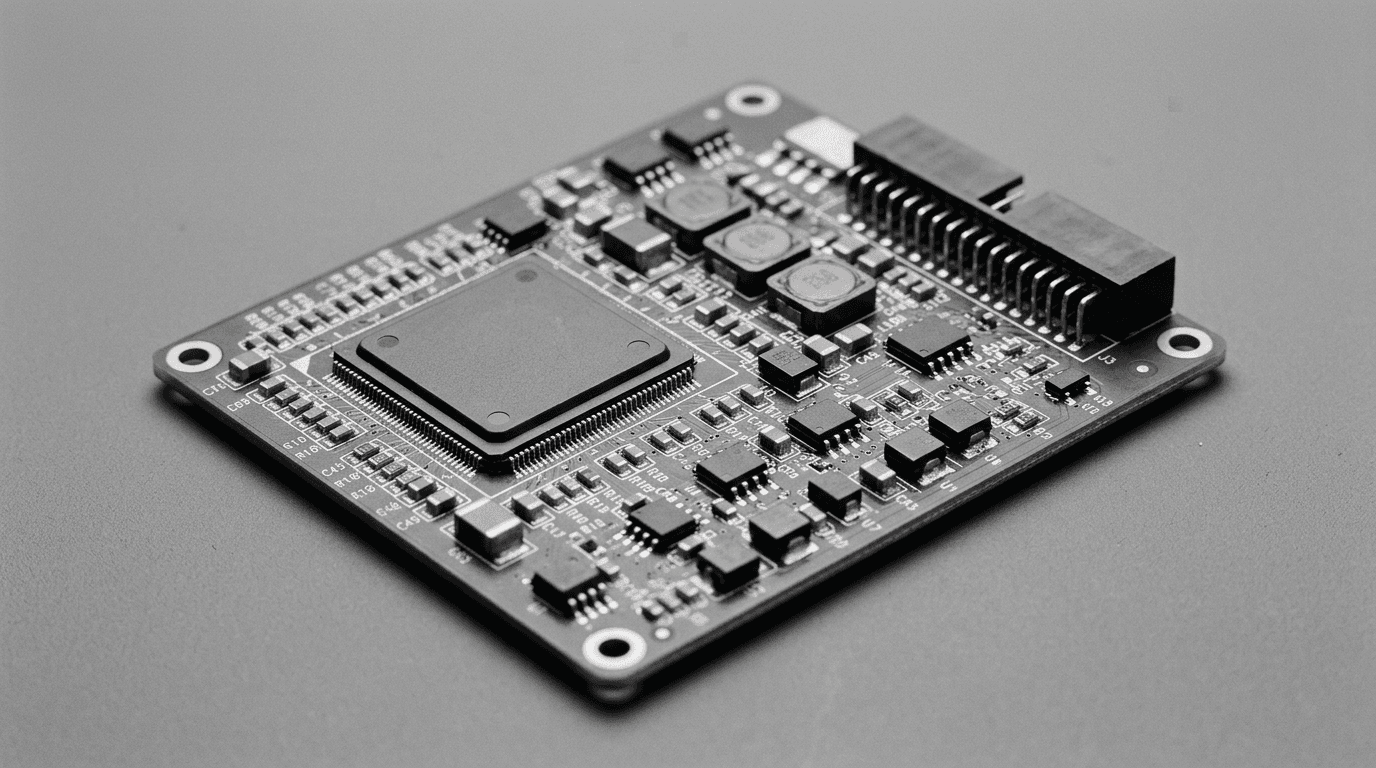
The OEM places the device onto a PCB and assembles it into a finished product. Every defect that escaped the previous 11 stages arrives here, and the cost to correct it is now at its maximum.
What happens at this stage
Incoming components are verified against the purchase specification. Solder paste is printed onto the board, components are placed by pick-and-place, and the assembly passes through reflow. Inspection runs at three points: solder paste inspection after printing, AOI after placement and after reflow, and X-ray for hidden joints under BGAs and QFNs.
For the OEM-side methods, see PCB visual inspection and automated X-ray inspection. Electronics assembly inspection is covered in depth on the AI for electronics manufacturing hub.
Where the lifecycle closes
A defect created at Stage 3 and missed at every gate since arrives at an OEM's SMT line as a component that solders correctly and fails functionally. This is the argument for distributed inspection rather than a single final gate: coverage at eight stages costs less than escape at one.
Deep dives3
- Incoming Component Inspection at OEMs — coming
- How Defects Affect End Product Reliability — coming
- PCB Assembly Inspection — coming
How AI Changes Inspection at Every Stage
Inspection hardware is not usually the constraint. Most fabs and back-end lines already own tools capable of resolving the defects they are missing. The constraint is the software deciding what the images mean.
Rule-based systems have three structural limits. They require a golden reference, so anything outside the reference set gets flagged or missed. They cannot separate nuisance from killer, because threshold sensitivity is a single dial trading escapes against false positives. And they do not improve, so a recipe tuned in January performs worse in June unless someone retunes it.
| Capability | What it does | Stages |
|---|---|---|
| Defect detection | Submicron defects at full sensitivity, near zero false positives | 3, 6, 7, 9 |
| Defect classification | Sorts defects by class so engineers see only what matters | 4, 7, 11 |
| Defect segmentation | Pixel-level boundaries for area, coverage and residue | 3, 7 |
| Defect review | Automated judgment and disposition at production volume | 4, 5, 9 |
| Defect monitoring | Continuous inline screening and drift detection across lots | 5, 8, 10 |
| Virtual metrology | Predicts measurement values from existing process data | 3, 4 |
| Advanced process control | Closes the loop from inspection output to recipe adjustment | 3, 4 |
| Labeling | Builds training sets from 20 to 40 images per defect class | All VI stages |
Three properties that matter for deployment
New defect classes need 20 to 40 labelled images, not thousands. A new package type is a days-long onboarding, not a quarter-long project.
The platform sits on top of existing AOI, SEM and optical tools. No hardware purchase, no rip and replace, no engineering resource writing integration code.
Fab image data is among the most sensitive IP a manufacturer holds. Deployment runs inside the customer environment, with no training on customer data without consent.
Inspection and Metrology Across the Full Lifecycle
Several capabilities run across stages rather than sitting inside one.
- Inspection versus metrology. Inspection finds unintended features, metrology measures intended ones. Semiconductor inspection and metrology explained.
- Quality control framework. Where gates sit, what the sampling plan is, how disposition decisions get made. Semiconductor quality control.
- Advanced process control. What is APC and FDC systems.
- Virtual metrology. Virtual metrology guide and AI in process control.
- Root cause analysis. Automated root cause analysis and preventing process drift.
- Data infrastructure. Defect data management and MES systems.
- Machine learning in inspection. Defect detection using machine learning, deep learning in semiconductor manufacturing and how AI is advancing semiconductor manufacturing.
- Legacy line automation. Legacy fab automation.
Semiconductor Inspection Equipment Landscape
The tool set breaks down by physics rather than by vendor.
| Method | Resolution | Throughput | Best for |
|---|---|---|---|
| Brightfield optical | ~20 nm sensitivity | High | Pattern defects on planar surfaces |
| Darkfield optical | ~20 nm sensitivity | High | Particles, defects on topography |
| Macro optical | 10 µm and up | Very high | Full-wafer signatures, handling damage |
| E-beam | Sub-10 nm | Very low | Voltage contrast, buried defects |
| CD-SEM | Sub-nm precision | Low | Critical dimension measurement |
| Scatterometry (OCD) | Sub-nm precision | High | Profile and film on periodic structures |
| X-ray / AXI | 1 µm and up | Medium | Hidden joints, voids, internal packaging |
| Acoustic microscopy | µm scale | Low | Delamination, internal voids |
For the buyer view: semiconductor inspection equipment, top wafer inspection tools, KLA defect inspection systems and Hitachi High-Tech inspection tools.
For industry context on who builds what and where: top 10 semiconductor foundries, top AI semiconductor companies and semiconductor manufacturing solutions.
Glossary
The terms that recur across the twelve stages, in plain language.
- Advanced process control (APC)
- Closed-loop control that adjusts process recipes based on metrology and inspection feedback, including run-to-run control and fault detection.
- AOI
- Automated optical inspection. Camera-based inspection comparing captured images against a reference to detect defects without operator judgment.
- Back end
- Assembly, packaging, test and shipping — everything after the wafer leaves the fab.
- Bevel
- The rounded edge profile of a wafer, shaped to resist chipping and particle generation during handling.
- Bin
- A category assigned to a die or device based on electrical test results, covering pass grades and specific failure modes.
- Bow and warp
- Deviation of a wafer from a flat plane. Bow is measured at the centre point, warp across the full surface.
- Burn-in
- Sustained voltage and temperature stress that surfaces infant-mortality failures before shipment.
- CD
- Critical dimension. The smallest controlled feature width on a layer, measured by CD-SEM or scatterometry.
- CMP
- Chemical mechanical polishing. A planarisation step combining chemical slurry and mechanical abrasion to flatten the wafer between layers.
- COP
- Crystal originated particle. A vacancy cluster formed during crystal growth that behaves like a sub-surface void and degrades gate oxide integrity.
- Czochralski process
- A crystal growth method in which a seed crystal is pulled from molten silicon to form a single-crystal ingot.
- Defect map
- The spatial plot of flagged sites on a wafer. Clustering often points at the process step that caused them.
- Die
- One individual chip on the wafer, separated at dicing.
- Escape
- A defective unit that passes an inspection gate and moves downstream undetected.
- False positive
- A good unit incorrectly flagged as defective. Also called an over-reject or nuisance defect.
- First pass yield
- The proportion of units passing all process and test steps without rework or repair.
- Flip chip
- An interconnect method in which the die is inverted and connected through solder bumps or copper pillars rather than wire bonds.
- Front end (FEOL/BEOL)
- Wafer fabrication — transistor and interconnect layers built by repeated litho, deposition and etch cycles.
- Ingot
- A single-crystal silicon cylinder grown from a melt, sliced into wafers.
- Kerf
- The material removed by the dicing cut, and the street width allocated for it.
- KGD (known good die)
- A die that has passed wafer probe and is cleared to enter packaging.
- Killer defect
- A defect large or positioned such that it causes electrical failure of the affected die.
- Metrology
- Measurement of intended dimensions and material properties, as distinct from inspection, which finds unintended features.
- MSL
- Moisture sensitivity level. A rating defining how long a package may be exposed to ambient humidity before reflow without risk of damage.
- Nuisance rate
- The share of flagged sites that are not real defects — the cost of running inspection at high sensitivity.
- Overlay
- Layer-to-layer alignment accuracy. Overlay error is the misregistration between a printed layer and the layer beneath it.
- Photomask
- The patterned quartz plate carrying the layout for one layer, projected onto the wafer during lithography. Also called a reticle.
- Popcorning
- Package cracking caused by absorbed moisture vaporising rapidly during reflow or burn-in.
- Probe card
- The interface carrying fine contacts that land on die pads to make electrical connection during wafer test.
- Segmentation
- Pixel-level classification of an image, producing defect boundaries and area rather than a bounding box or a pass/fail call.
- Singulation
- Separating a finished wafer into individual dies, by blade, laser or plasma dicing.
- TSV
- Through-silicon via. A vertical electrical connection passing through a die, enabling 3D stacked packaging.
- TTV
- Total thickness variation. The difference between the maximum and minimum thickness of a wafer.
- Virtual metrology
- Prediction of measurement values from process and sensor data, used to raise sampling coverage without additional metrology capacity.
- Voltage contrast
- An e-beam technique revealing electrical opens and shorts through differences in secondary electron emission.
- Wafer
- The thin silicon disc that carries every die through front-end processing. 300 mm is the volume standard.
- Wafer probe / sort
- Electrical test of each die while still on the wafer, before dicing.
- Yield
- The proportion of manufactured units meeting specification. Reported at die level, wafer level and line level.
FAQs
The process runs across 12 stages from silicon ingot to integration into final products. Within Stage 3 alone, an advanced logic node executes over 1,000 individual process steps across 50 to 100 mask layers, since each layer repeats the deposition, lithography, etch and planarisation cycle.
Front-end fabrication typically takes 8 to 16 weeks depending on node complexity and layer count. Back-end assembly, test and packaging add a further 2 to 4 weeks. Total cycle time from bare wafer to shipped device commonly runs 3 to 6 months including queue time.
Eight of the 12 stages carry a visual inspection gate: wafer fabrication, inspection and metrology, wafer probe, dicing, die attach and packaging, final test and burn-in, marking, and carrier packing. Stages 1, 2, 11 and 12 use measurement, authentication or electrical methods instead.
Inspection finds features that should not be present, such as particles, scratches and bridges. Metrology measures features that should be present, such as line width, overlay alignment and film thickness. Both run between process steps and both feed the same process control loops. More detail.
Wafer fabrication produces the highest defect count, because it repeats hundreds of process cycles and each cycle can introduce particles, pattern defects and planarisation damage. Advanced packaging produces the widest defect variety, because it combines materials, thermal processes and fine-pitch interconnect in one flow.
Cost rises roughly tenfold per stage downstream. A defect caught inline costs a rework cycle. The same defect caught at final test has consumed the full fabrication, dicing, packaging and test cost of the die. Reaching the field, it becomes a warranty or recall cost.
No, and it should not. Averroes AI runs as a software overlay on installed AOI, optical and SEM tools, reading the images those tools already produce. The hardware stays. What changes is the accuracy of the decision made on each image. More detail.
Averroes AI reaches production accuracy with 20 to 40 labelled images per defect class using few shot learning, rather than the thousands of examples conventional deep learning approaches require. Active learning then improves the model from operator dispositions during production.
A false positive is a good unit flagged as defective. They cost yield through unnecessary scrap and cost engineering hours through manual review. High false positive rates also drive operators to loosen thresholds, which is the most common route to genuine escapes.
Virtual metrology predicts measurement values from process and sensor data instead of physically measuring each wafer. It applies at Stages 3 and 4, raising effective sampling toward full coverage without adding metrology tool capacity. More detail.
Inspect every stage without replacing your tools
Eight inspection gates, one platform, no new hardware. Averroes AI reads the images your existing tools already capture, holds near zero false positives at full sensitivity, and deploys on premise in days.