Known Good Die (KGD): How Dies Are Tested, Inspected and Mapped Before Packaging
Averroes
Nov 11, 2026
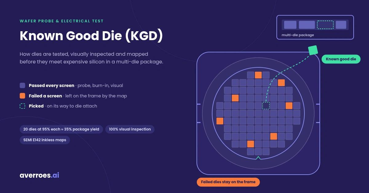
A known good die (KGD) is a bare, unpackaged die tested and inspected to the same quality and reliability as an equivalent packaged part. It passes wafer probe test, any further die-level test or burn-in, and a visual inspection after dicing, and its map position tells the pick tool which dies to take. KGD matters most in multi-die packages, where one bad die can scrap every good die assembled with it.
Known good die sits at the end of Stage 05 of the semiconductor manufacturing process, where tested wafers are handed off to dicing and die attach. This guide from Averroes.ai, an AI visual inspection platform for manufacturers, covers what KGD means, why multi-die packaging depends on it, how a die earns the label, and where visual inspection and wafer maps fit.
Key Notes
KGD has no single definition: MIL-PRF-38534 calls it a bare die equal in quality to an equivalent packaged die; MIL-PRF-38535 does not define it.
Multi-die yield multiplies: twenty dies at 95% each give a module first pass test yield of about 35%.
Visual inspection is part of KGD: military die classes require 100% visual inspection of die alongside 100% electrical test.
The map decides which dies ship: inkless maps under SEMI E142 tell the pick tool which dies are good.
What Is a Known Good Die?
A known good die is a bare die that has been tested and screened until there is very high confidence it will work, and keep working, as well as the same chip would in its own package. The die is still unpackaged. What makes it “known good” is the evidence behind it, not its physical form.
The term does not have one fixed meaning. A NASA parts bulletin notes that KGD means different things to different suppliers. MIL-PRF-38535, the military specification for microcircuits, does not define it at all. MIL-PRF-38534, which covers hybrid microcircuits, defines KGD as a bare die of the same quality and reliability level as an equivalent packaged die. Patent literature frames it the same way, as a die with very high confidence that it will operate reliably over its lifetime.
Bare die vs probed die vs known good die
Die State
What It Has Passed
What a Buyer Can Rely On
Bare die
Nothing claimed beyond singulation
Physical form only
Probed die
Wafer probe test
Worked at probe conditions
Known good die
Probe, further test or burn-in, visual inspection, traceable map record
Quality equal to a packaged part
“Bare die” and “known good die” are often used loosely together. A bare die is a physical form; a known good die is a quality claim about it. The claim is only as strong as the screening behind it, which is why buyers ask what “known good” covered before they accept a lot. The screening runs mostly in the wafer probe and electrical test stage, with visual inspection after dicing.
Why Multi-Die Packages Need Known Good Die
Multi-die packages need known good die because package yield is the product of every die’s yield. A single-die package that contains a bad die loses one die. A package with ten or twenty dies loses all of them, plus the substrate and the assembly work, when one die fails.
The arithmetic is unforgiving. Patent literature on KGD testing notes that a multi-chip module’s test yield is at best the product of its individual die yields: ten dies at 95% each give 59.8% at most. Another patent puts twenty dies at 95% yield at a first pass module test yield of only 35%. The table shows the same calculation across die counts.
Package yield when every die is 95% good
Dies per Package
Package Yield at 95% per Die
Package Yield at 99% per Die
2
90.3%
98.0%
4
81.5%
96.1%
8
66.3%
92.3%
10
59.9%
90.4%
20
35.8%
81.8%
Values are per-die yield raised to the die count, before any assembly losses.
Chiplets and 2.5D or 3D integration make this worse. An Open Compute Project paper on system-in-package testing states that in a multi-die package, one bad die can fail the whole package. Cost models agree on where the money goes. A 2025 cost analysis tool for chiplet systems found that when test coverage is too low, good dies are scrapped along with the assemblies that hold an undetected bad die. An earlier chiplet cost model counted the KGDs wasted by packaging defects as a significant share of total cost when die cost is high. The same pressures shape advanced packaging metrology.
There is a second effect. Dies for 2.5D and 3D stacks are thinned, and the Open Compute paper notes that thinning raises the probability of mechanical damage. A thin die that tested good can still crack or chip before it is bonded, and an electrical test that ran before dicing will not see it.
The takeaway: the more dies in a package, the more each die’s screening is worth.
How a Die Becomes Known Good
A die becomes known good by passing a sequence of electrical, stress and visual screens, each recorded against its position on the wafer so the right dies are picked for assembly. The exact screens depend on the product and the customer, but the sequence below is the common shape.
A die becomes known good in 5 steps:
Wafer probe test. Every die on the finished wafer is tested electrically and given a bin code, as described in wafer probe test. Dies that fail are excluded from here on.
Further test or burn-in. Some products need screening that probing alone cannot provide, such as burn-in to catch early-life failures or full-speed testing. This can run at wafer level or on individual dies held in temporary carriers, as patent literature on discrete die burn-in describes. The wider picture of stress testing is covered in semiconductor reliability testing.
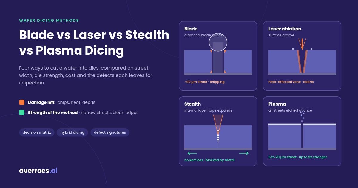
Dicing. The wafer is cut into individual dies on a film frame. Dicing can chip edges and start cracks, the subject of wafer dicing inspection and crack inspection.
Visual inspection. Singulated dies are inspected for damage that electrical test cannot see: chips, cracks, scratches, contamination and pad damage. How the images are captured and processed is covered in die inspection.
Map-driven die selection. A die sorter or pick-and-place tool reads the wafer map and picks only the dies that passed every screen, for die attach or for shipping as bare die.
The takeaway: each step catches what the one before it cannot, and the map carries every result to the pick.
Inkless Wafer Maps and SEMI E142
An inkless wafer map is a digital record of every die’s bin result, used by downstream tools to decide which dies to pick, in place of physical ink dots on the failing dies. Older lines marked bad dies with ink so an operator or a vision system could skip them. The first process substrate maps were built to support was this inkless binning.
The map carries a bin value for each die position: for example, 1 for a good die, 10 for an open and 11 for a short. SEMI E142, approved in 2005, defines how these substrate maps are reported, stored and transmitted between sites. It covers several substrate types, including wafers, film frames, strips and trays, and holds bin code maps as overlays. The standard also supports transfer maps that trace each die on a strip or tray back to its original wafer position, so a field failure can be followed back to the wafer it came from.
When the Map and the Dies Disagree
A wafer map is only useful if its coordinates match the physical dies on the frame. The map was written at probe test, often in another building; the dies are picked after dicing and frame mounting. Substrate mapping uses a reference die to align the two, and every coordinate is ultimately referenced to the wafer notch, as explained in wafer notch orientation. If the map is rotated or offset by one die, the pick tool takes failed dies and leaves good ones on the frame, and nothing in the map itself shows the error. A visual check of the frame against the map, at the reference die and at known fail positions, is what catches it.
“Die sorter” here means the tool that picks dies by bin from a diced frame. It is a different thing from wafer sort, which is the electrical test that produced the bins.
The takeaway: the map carries the decision, so its alignment to the physical dies has to be verified, not assumed.
What Visual Inspection Adds to Known Good Die
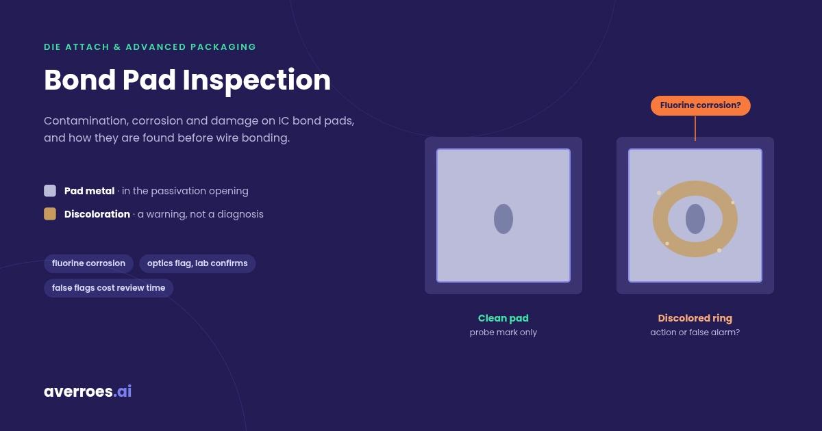
Visual inspection adds the defects that electrical test cannot see but that still threaten bonding or long-term reliability. A die with a chipped edge, a crack that has not yet reached the active area, contamination on a pad or a scratch across the passivation can pass every electrical test and still fail at die attach or in the field.
That is why high-reliability die classes treat inspection as part of the definition. The NASA bulletin describes military die classes screened with 100% electrical test, 100% visual inspection of die, and additional screening. MIL-STD-883 Method 2010, the internal visual inspection method for monolithic microcircuits, sets out the criteria: it checks internal materials, construction and workmanship under both high and low magnification. For dies mounted upside down, as in flip-chip assembly, the criteria that cannot be checked after mounting must be inspected before die attach.
Thin dies raise the stakes again. Thinning for 2.5D and 3D stacks makes dies more prone to mechanical damage, so the gap between “tested good” and “still good at bonding” widens.
The defects themselves are covered in detail elsewhere in the hub:
AI classification separates die-level defects that threaten function or bonding from cosmetic marks, so reviewers spend their time on the dies that actually need a decision. Visual screening of every die produces a large volume of images, and most flagged dies are either clearly fine or clearly bad. The cost sits in the borderline ones.
AI does three jobs in KGD screening:
Classify die images into real defect classes, such as chips, cracks, pad damage and contamination, and separate them from cosmetic marks that do not affect function.
Route borderline dies to human review with the classification attached, so an engineer confirms the call instead of starting from scratch.
Trend die-level defect classes by wafer, lot and dicing tool, so a rising chipping rate points to a saw or blade before it fills a frame with rejects.
Averroes.ai classifies die-level defects from the inspection images a fab or assembly site already captures, using AI defect classification. It trains models from 20 to 40 labeled images per defect class, with no code, and deploys on premise so die images stay inside the customer environment. AI defect review then puts borderline dies in front of engineers with the model’s call attached. Averroes is not a tester, sorter or inspection tool: it works on the images those tools produce.
Is Every Die You Ship Known Good?
Test AI defect review on your own die inspection images
Frequently Asked Questions
What is the difference between a bare die and a known good die?
A bare die is any unpackaged die cut from a wafer, with no claim about its quality. A known good die is a bare die that has passed probe test, any further test or burn-in, and visual inspection, so its quality matches an equivalent packaged part. Bare die describes the form; known good die describes the evidence.
What is KGD testing?
KGD testing is the screening that turns a bare die into a known good die. It starts with wafer probe test and can add burn-in, full-speed or temperature testing at wafer level or in temporary die carriers. Visual inspection after dicing completes it, and every result is recorded against the die’s position on the wafer map.
Why is known good die important for chiplets?
Chiplet packages combine several dies, so package yield is the product of every die’s yield. One bad die can fail the whole package and scrap the good dies, interposer and memory bonded with it. Twenty dies at 95% each give only about 35% first pass yield, so screening each die first is far cheaper.
What is an inkless wafer map?
An inkless wafer map is a digital file that records each die’s bin result, such as pass, open or short, by its position on the wafer. Pick-and-place and die sorter tools read it to take only good dies. It replaced the older practice of marking failed dies with ink dots.
What is SEMI E142?
SEMI E142 is the industry standard for substrate maps, approved in 2005. It defines how die-level maps of wafers, film frames, strips and trays are reported, stored and transmitted between sites, including bin code maps. It also supports transfer maps that trace each packaged die back to its original wafer position.
What is MIL-STD-883 Method 2010?
MIL-STD-883 Method 2010 is the internal visual inspection method for monolithic microcircuits. It checks internal materials, construction and workmanship under high and low magnification. For dies mounted upside down, such as flip-chip parts, criteria that cannot be inspected after mounting must be checked before die attach.







A known good die (KGD) is a bare, unpackaged die tested and inspected to the same quality and reliability as an equivalent packaged part. It passes wafer probe test, any further die-level test or burn-in, and a visual inspection after dicing, and its map position tells the pick tool which dies to take. KGD matters most in multi-die packages, where one bad die can scrap every good die assembled with it.
Known good die sits at the end of Stage 05 of the semiconductor manufacturing process, where tested wafers are handed off to dicing and die attach. This guide from Averroes.ai, an AI visual inspection platform for manufacturers, covers what KGD means, why multi-die packaging depends on it, how a die earns the label, and where visual inspection and wafer maps fit.
Key Notes
What Is a Known Good Die?
A known good die is a bare die that has been tested and screened until there is very high confidence it will work, and keep working, as well as the same chip would in its own package. The die is still unpackaged. What makes it “known good” is the evidence behind it, not its physical form.
The term does not have one fixed meaning. A NASA parts bulletin notes that KGD means different things to different suppliers. MIL-PRF-38535, the military specification for microcircuits, does not define it at all. MIL-PRF-38534, which covers hybrid microcircuits, defines KGD as a bare die of the same quality and reliability level as an equivalent packaged die. Patent literature frames it the same way, as a die with very high confidence that it will operate reliably over its lifetime.
Bare die vs probed die vs known good die
“Bare die” and “known good die” are often used loosely together. A bare die is a physical form; a known good die is a quality claim about it. The claim is only as strong as the screening behind it, which is why buyers ask what “known good” covered before they accept a lot. The screening runs mostly in the wafer probe and electrical test stage, with visual inspection after dicing.
Why Multi-Die Packages Need Known Good Die
Multi-die packages need known good die because package yield is the product of every die’s yield. A single-die package that contains a bad die loses one die. A package with ten or twenty dies loses all of them, plus the substrate and the assembly work, when one die fails.
The arithmetic is unforgiving. Patent literature on KGD testing notes that a multi-chip module’s test yield is at best the product of its individual die yields: ten dies at 95% each give 59.8% at most. Another patent puts twenty dies at 95% yield at a first pass module test yield of only 35%. The table shows the same calculation across die counts.
Package yield when every die is 95% good
Values are per-die yield raised to the die count, before any assembly losses.
Chiplets and 2.5D or 3D integration make this worse. An Open Compute Project paper on system-in-package testing states that in a multi-die package, one bad die can fail the whole package. Cost models agree on where the money goes. A 2025 cost analysis tool for chiplet systems found that when test coverage is too low, good dies are scrapped along with the assemblies that hold an undetected bad die. An earlier chiplet cost model counted the KGDs wasted by packaging defects as a significant share of total cost when die cost is high. The same pressures shape advanced packaging metrology.
There is a second effect. Dies for 2.5D and 3D stacks are thinned, and the Open Compute paper notes that thinning raises the probability of mechanical damage. A thin die that tested good can still crack or chip before it is bonded, and an electrical test that ran before dicing will not see it.
The takeaway: the more dies in a package, the more each die’s screening is worth.
How a Die Becomes Known Good
A die becomes known good by passing a sequence of electrical, stress and visual screens, each recorded against its position on the wafer so the right dies are picked for assembly. The exact screens depend on the product and the customer, but the sequence below is the common shape.
A die becomes known good in 5 steps:
The takeaway: each step catches what the one before it cannot, and the map carries every result to the pick.
Inkless Wafer Maps and SEMI E142
An inkless wafer map is a digital record of every die’s bin result, used by downstream tools to decide which dies to pick, in place of physical ink dots on the failing dies. Older lines marked bad dies with ink so an operator or a vision system could skip them. The first process substrate maps were built to support was this inkless binning.
The map carries a bin value for each die position: for example, 1 for a good die, 10 for an open and 11 for a short. SEMI E142, approved in 2005, defines how these substrate maps are reported, stored and transmitted between sites. It covers several substrate types, including wafers, film frames, strips and trays, and holds bin code maps as overlays. The standard also supports transfer maps that trace each die on a strip or tray back to its original wafer position, so a field failure can be followed back to the wafer it came from.
When the Map and the Dies Disagree
A wafer map is only useful if its coordinates match the physical dies on the frame. The map was written at probe test, often in another building; the dies are picked after dicing and frame mounting. Substrate mapping uses a reference die to align the two, and every coordinate is ultimately referenced to the wafer notch, as explained in wafer notch orientation. If the map is rotated or offset by one die, the pick tool takes failed dies and leaves good ones on the frame, and nothing in the map itself shows the error. A visual check of the frame against the map, at the reference die and at known fail positions, is what catches it.
“Die sorter” here means the tool that picks dies by bin from a diced frame. It is a different thing from wafer sort, which is the electrical test that produced the bins.
The takeaway: the map carries the decision, so its alignment to the physical dies has to be verified, not assumed.
What Visual Inspection Adds to Known Good Die
Visual inspection adds the defects that electrical test cannot see but that still threaten bonding or long-term reliability. A die with a chipped edge, a crack that has not yet reached the active area, contamination on a pad or a scratch across the passivation can pass every electrical test and still fail at die attach or in the field.
That is why high-reliability die classes treat inspection as part of the definition. The NASA bulletin describes military die classes screened with 100% electrical test, 100% visual inspection of die, and additional screening. MIL-STD-883 Method 2010, the internal visual inspection method for monolithic microcircuits, sets out the criteria: it checks internal materials, construction and workmanship under both high and low magnification. For dies mounted upside down, as in flip-chip assembly, the criteria that cannot be checked after mounting must be inspected before die attach.
Thin dies raise the stakes again. Thinning for 2.5D and 3D stacks makes dies more prone to mechanical damage, so the gap between “tested good” and “still good at bonding” widens.
The defects themselves are covered in detail elsewhere in the hub:
Where AI Fits in Known Good Die Screening
AI classification separates die-level defects that threaten function or bonding from cosmetic marks, so reviewers spend their time on the dies that actually need a decision. Visual screening of every die produces a large volume of images, and most flagged dies are either clearly fine or clearly bad. The cost sits in the borderline ones.
AI does three jobs in KGD screening:
Averroes.ai classifies die-level defects from the inspection images a fab or assembly site already captures, using AI defect classification. It trains models from 20 to 40 labeled images per defect class, with no code, and deploys on premise so die images stay inside the customer environment. AI defect review then puts borderline dies in front of engineers with the model’s call attached. Averroes is not a tester, sorter or inspection tool: it works on the images those tools produce.
Is Every Die You Ship Known Good?
Test AI defect review on your own die inspection images
Frequently Asked Questions
What is the difference between a bare die and a known good die?
A bare die is any unpackaged die cut from a wafer, with no claim about its quality. A known good die is a bare die that has passed probe test, any further test or burn-in, and visual inspection, so its quality matches an equivalent packaged part. Bare die describes the form; known good die describes the evidence.
What is KGD testing?
KGD testing is the screening that turns a bare die into a known good die. It starts with wafer probe test and can add burn-in, full-speed or temperature testing at wafer level or in temporary die carriers. Visual inspection after dicing completes it, and every result is recorded against the die’s position on the wafer map.
Why is known good die important for chiplets?
Chiplet packages combine several dies, so package yield is the product of every die’s yield. One bad die can fail the whole package and scrap the good dies, interposer and memory bonded with it. Twenty dies at 95% each give only about 35% first pass yield, so screening each die first is far cheaper.
What is an inkless wafer map?
An inkless wafer map is a digital file that records each die’s bin result, such as pass, open or short, by its position on the wafer. Pick-and-place and die sorter tools read it to take only good dies. It replaced the older practice of marking failed dies with ink dots.
What is SEMI E142?
SEMI E142 is the industry standard for substrate maps, approved in 2005. It defines how die-level maps of wafers, film frames, strips and trays are reported, stored and transmitted between sites, including bin code maps. It also supports transfer maps that trace each packaged die back to its original wafer position.
What is MIL-STD-883 Method 2010?
MIL-STD-883 Method 2010 is the internal visual inspection method for monolithic microcircuits. It checks internal materials, construction and workmanship under high and low magnification. For dies mounted upside down, such as flip-chip parts, criteria that cannot be inspected after mounting must be checked before die attach.