Wafer Dicing: How Wafers Are Cut Into Dies and How Dicing Defects Are Caught
Averroes
Nov 12, 2026
Wafer dicing is the step that cuts a finished, tested wafer into individual dies. The wafer is mounted on dicing tape in a frame, then cut along the streets between dies by a diamond blade, a laser or a plasma etch. Each method leaves its own damage, from chipped edges to heat damage. Post-dicing inspection catches damaged dies before die attach, and AI visual inspection platforms such as Averroes.ai classify that damage from existing inspection images.
Wafer dicing is Stage 06 of the semiconductor manufacturing process, between wafer probe test and die attach. This guide from Averroes.ai, an AI visual inspection platform for manufacturers, covers how dicing works, what each method leaves behind, the defects that matter, and how they are inspected.
Key Notes
Every method leaves a signature: blades chip and crack, ablation lasers leave heat damage and debris, stealth and plasma dicing leave far less.
Blade wear shows up twice: a worn blade both chips edges and drifts off the street center.
Chipping is still often measured by hand: engineers draw measurement lines across each wafer quadrant on an optical tool.
Faster is not always worse: one 2025 study improved back chipping Cpk from 1.26 to 1.76 while raising capacity 11.9%.
What Is Wafer Dicing?
Wafer dicing is a back-end process that separates a processed semiconductor wafer into individual dies by cutting along the lanes reserved between them, used to prepare tested dies for die attach and packaging. It is also called wafer singulation or die singulation. Dicing comes after wafer probe test, which has already recorded which dies work, and before die attach, where good dies go into packages.
Dicing is where a wafer’s value is most exposed to mechanical damage. Every die on the wafer has been fabricated and tested by this point, so a chip or crack introduced here destroys a die that was already paid for in full. In multi-die packages, a damaged die that slips through can scrap the whole assembly, which is why dicing quality is part of what makes a known good die.
The wafer dicing stage usually follows backgrinding, which thins the wafer to its final thickness. Some flows reverse that order and cut before grinding, a method called dicing before grinding (DBG).
What Are Dicing Streets, Scribe Lines and Kerf?
TA dicing street is the lane reserved between dies on a wafer layout, used as the path for the dicing cut. Three terms describe the geometry of the cut, and they are often confused:
Dicing street: the lane reserved between dies on the wafer layout, where cutting is allowed.
Scribe line: the same lane, often carrying test structures and alignment marks used during fabrication.
Kerf: the material actually removed by the cut. Kerf width is how wide that removed strip is.
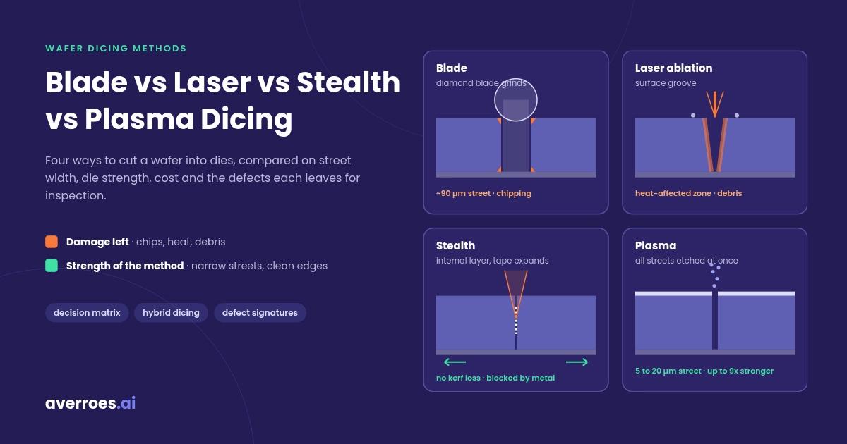
Kerf width decides how much wafer area is spent on cutting rather than on dies. A paper by ON Semiconductor and Plasma-Therm, presented at the 228th ECS Meeting in October 2015, compared saw streets of about 90 µm with plasma dicing streets of 5 to 20 µm. Narrower streets mean more dies per wafer, which is one reason dicing method choice is a cost decision as well as a quality one.
How Does the Wafer Dicing Process Work?
The wafer dicing process is a back-end sequence that mounts, cuts, cleans and inspects a thinned wafer, used to deliver separated dies held in place on tape for pick. The exact cut depends on the method, but the surrounding steps are common to all of them.
The wafer dicing process runs in 6 steps:
Mount. The wafer is placed on dicing tape stretched across a film frame. The tape holds every die in position once it is separated.
Align. The dicing machine finds the streets using alignment marks and sets its cut path.
Cut. A diamond blade, a laser or a plasma etch separates the dies along every street.
Clean. Debris and slurry are removed from the frame. Dry methods need little or no cleaning.
Inspect. The kerf and die edges are checked for chips, cracks and cut position.
Expand or hand off. The tape is stretched to open gaps between dies, or the frame goes straight to die pick.
A wafer dicing machine, called a dicing saw when it uses a blade, aligns the wafer and makes the cuts. A dicing blade is a thin diamond wheel that grinds through the silicon at high speed.
Dicing before grinding. Most wafers are thinned first and diced after (dicing after grinding, DAG). In dicing before grinding (DBG), the dies are defined by a partial cut from the front, then the wafer is ground from the back until the dies separate. A 2016 DISCO technical review reports that DBG greatly reduces backside chipping, because grinding removes the damaged layer the half-cut leaves on the backside.
The takeaway: the cut is one step of six, and inspection sits between the cut and the pick.
What Damage Does Each Dicing Method Leave Behind?
A dicing method is the separation technique that cuts the wafer into dies, and each one leaves its own damage signature, used to decide what post-dicing inspection must look for. Choosing a method is a broader decision, covered in wafer dicing methods. This section covers only what each method leaves on the die, because that is what inspection has to find.
Blade. A diamond blade grinds through the street. Hamamatsu’s comparison of dicing technologies lists the problems: stress and recontamination from vibration and cooling water, loss of die strength from chipping, and scattered debris that can damage fragile structures. Blade dicing remains the most widely used method.
Laser ablation. A laser focused on the surface vaporizes a groove through the street. That leaves a heat-affected zone that weakens the die, and molten debris and microcracks along the cut, as a Photonics.com article on dicing describes.
Stealth dicing. A laser at a wavelength silicon transmits is focused inside the wafer, forming a modified layer, and the tape is then expanded so cracks run from that layer to both surfaces. Hamamatsu describes the result as having no kerf loss and no chipping on the top and bottom surfaces of the chip.
Plasma dicing. A dry etch removes the street chemically, cutting all streets at once. KLA’s August 2022 overview of plasma dicing says it causes no mechanical damage or heat-affected zone and gives higher die break strength, which matters as industry roadmaps push die thickness below 50 µm.
Dicing defects by method
Method
How It Separates the Die
Typical Damage
What Inspection Looks For
Blade
Diamond blade grinds the street
Chipping, cracks, debris
Chip size, cracks, kerf position
Laser ablation
Laser vaporizes a surface groove
Heat-affected zone, microcracks, debris
Debris, edge discoloration, cracks
Stealth
Internal laser layer, then tape expansion
Little surface damage
Incomplete separation, edge cracks
Plasma
Dry etch removes the street
Little mechanical damage
Incomplete etch, residue
Low-k dielectric stacks are a special case. Photonics.com notes that conventional dicing of low-k wafers causes chipping, debris and delamination along with wide kerfs, which is one reason fragile stacks move to stealth or plasma dicing. The same pressure on thin and fragile dies runs through advanced packaging metrology.
The takeaway: the method sets which defects inspection must be tuned to find.
What Are Dicing Defects? Chipping, Cracks and Kerf Errors
Dicing defects are damage to a die’s edge, sidewall or surface caused by the cut, plus errors in where the cut runs and how wide it is, used as the accept or reject criteria before die attach. Chipping is the most common, because removing brittle silicon by force breaks small pieces off the edge of the groove.
What Is the Difference Between Topside and Backside Chipping?
Topside chipping is edge damage on the front, device side of the die, closest to the circuitry. Backside chipping is edge damage on the bottom of the die; patent literature describes it as fine cracks that form at the interface between the silicon and the dicing tape. DISCO notes that front and backside chipping both affect die strength, and that backside chipping tends to increase as wafers get thinner. Backside chips are also hard to see from the front. Both can start cracks that grow later, under thermal or mechanical stress; methods for finding cracks are covered in crack inspection.
How Does Blade Wear Cause Chipping and Kerf Drift?
Blade wear is the gradual loss of a dicing blade’s cutting edge and shape, and it damages dicing quality in two ways at once. A dicing apparatus patent explains that as the blade wears, chipping increases, and the blade’s center drifts away from the street center because of heat deformation. A worn blade both chips edges and cuts in the wrong place. Because wear builds gradually, both effects grow wafer by wafer, which is why trending chipping by blade with defect monitoring catches a failing blade before it fills a frame with rejects.
Does Faster Dicing Mean More Chipping?
Feed speed is the speed at which the wafer moves into the dicing blade, and it sets both throughput and chipping. The usual assumption is that faster feed speed means more chipping, so throughput and quality trade against each other. A 2025 study presented at the 32nd ASEMEP National Technical Symposium found otherwise for the silicon wafers and blades it tested. Standard feed speeds sit around 20 to 60 mm/s; new high feed-speed parameters eliminated a recurring triangular chip-out issue and improved back chipping Cpk from 1.26 to 1.76, while raising capacity by 11.9%. The lesson is not that faster is always better, but that chipping responds to the whole parameter set, and only measured chipping data shows which way a change moves it.
The takeaway: chipping is a moving quantity, driven by wear and parameters, so it has to be measured continuously.
How Are Dicing Defects Inspected?
Dicing inspection is the check of kerf position, kerf width and die edges for chips and cracks, used to stop damaged dies before die pick. It happens at two points: at the dicing saw during cutting, and on the frame after dicing.
At the saw. Dicing machines check the kerf as they cut. The dicing apparatus patent describes the machine imaging the kerf with a camera to determine its position and width and whether chipping has occurred, or an operator checking it by sight. This catches blade wear and drift early, but only on the streets it samples.
After dicing. The whole frame is inspected optically for chipped, cracked or contaminated dies before the dies are picked. How these images are captured and processed is covered in die inspection.
Both checkpoints share the same weakness: measurement. A recent patent on automatic inspection of diced wafers states that detecting and measuring chipping is still a manual process, with a process engineer drawing measurement lines on an optical tool across each quadrant of the wafer. An earlier patent on evaluating dicing processes describes visual inspection of diced dies as time consuming, expensive and not entirely reliable, and notes that not all dies are inspected because there are so many.
Still Measuring Chipping by Hand?
Test AI defect detection on your own post-dicing images
Where Does AI Fit in Dicing Inspection?
AI dicing inspection is image-based detection that separates real chips and cracks from harmless dicing artifacts at micron scale, used on every die rather than a sample. The images already exist: dicing saws image the kerf, and post-dicing inspection images the frame. What is missing is consistent measurement and classification at production volume.
AI does three jobs in dicing inspection:
Detect and size chipping on kerf and frame images, on every street and every die edge instead of the quadrants an engineer has time to measure.
Classify what it finds into chips, cracks, debris and harmless marks within the allowed zone, so only real defects reach review.
Trend defect classes by blade, saw and lot, so rising chipping on one blade shows up as a trend before it becomes a yield loss.
Averroes.ai runs AI defect detection on the images the dicing saw camera and post-dicing inspection already capture. It trains models from 20 to 40 labeled images per defect class, with no code, and deploys on premise so wafer images stay inside the fab or assembly site. Averroes is not a dicing tool or a metrology system: it works on the images those tools produce. You can test AI defect detection on your own post-dicing images before committing to a deployment.
Frequently Asked Questions
What is the difference between wafer dicing and wafer singulation?
There is no practical difference. Wafer dicing and wafer singulation, also called die singulation, both mean separating a processed wafer into individual dies. “Dicing” is often used for the cutting step itself, while “singulation” describes the outcome: single dies ready for pick and die attach.
What is kerf width in wafer dicing?
Kerf width is the width of material removed by the dicing cut. It sets how much wafer area is spent on cutting rather than on dies. A 2015 ECS paper by ON Semiconductor and Plasma-Therm compared saw streets of about 90 µm with plasma dicing streets of 5 to 20 µm, so narrower kerfs fit more dies per wafer.
What causes chipping in wafer dicing?
Chipping happens because dicing removes brittle silicon by force, which breaks small pieces off the edges of the cut. Blade wear increases it, and so can feed speed and blade grit. Topside chipping damages the device-side edge; backside chipping damages the bottom edge and weakens the die, especially as wafers get thinner.
Which dicing method causes the least damage?
Stealth and plasma dicing cause the least surface damage. Stealth dicing forms a modified layer inside the wafer and separates dies by tape expansion, with no chipping on the top or bottom surface. Plasma dicing etches the streets chemically, with no mechanical damage or heat-affected zone.
What is dicing before grinding?
Dicing before grinding (DBG) reverses the usual order. The dies are defined by a partial cut from the front of the full-thickness wafer, then the wafer is ground from the back until the dies separate. Grinding removes the damaged layer the half-cut leaves, which greatly reduces backside chipping.
How is chipping measured after dicing?
Chipping is measured from images of the kerf and die edges, either by the dicing machine’s camera during cutting or by optical inspection of the frame afterward. In many lines an engineer still measures it manually on an optical tool, sampling quadrants of the wafer rather than every die.







Wafer dicing is the step that cuts a finished, tested wafer into individual dies. The wafer is mounted on dicing tape in a frame, then cut along the streets between dies by a diamond blade, a laser or a plasma etch. Each method leaves its own damage, from chipped edges to heat damage. Post-dicing inspection catches damaged dies before die attach, and AI visual inspection platforms such as Averroes.ai classify that damage from existing inspection images.
Wafer dicing is Stage 06 of the semiconductor manufacturing process, between wafer probe test and die attach. This guide from Averroes.ai, an AI visual inspection platform for manufacturers, covers how dicing works, what each method leaves behind, the defects that matter, and how they are inspected.
Key Notes
What Is Wafer Dicing?
Wafer dicing is a back-end process that separates a processed semiconductor wafer into individual dies by cutting along the lanes reserved between them, used to prepare tested dies for die attach and packaging. It is also called wafer singulation or die singulation. Dicing comes after wafer probe test, which has already recorded which dies work, and before die attach, where good dies go into packages.
Dicing is where a wafer’s value is most exposed to mechanical damage. Every die on the wafer has been fabricated and tested by this point, so a chip or crack introduced here destroys a die that was already paid for in full. In multi-die packages, a damaged die that slips through can scrap the whole assembly, which is why dicing quality is part of what makes a known good die.
The wafer dicing stage usually follows backgrinding, which thins the wafer to its final thickness. Some flows reverse that order and cut before grinding, a method called dicing before grinding (DBG).
What Are Dicing Streets, Scribe Lines and Kerf?
TA dicing street is the lane reserved between dies on a wafer layout, used as the path for the dicing cut. Three terms describe the geometry of the cut, and they are often confused:
Kerf width decides how much wafer area is spent on cutting rather than on dies. A paper by ON Semiconductor and Plasma-Therm, presented at the 228th ECS Meeting in October 2015, compared saw streets of about 90 µm with plasma dicing streets of 5 to 20 µm. Narrower streets mean more dies per wafer, which is one reason dicing method choice is a cost decision as well as a quality one.
How Does the Wafer Dicing Process Work?
The wafer dicing process is a back-end sequence that mounts, cuts, cleans and inspects a thinned wafer, used to deliver separated dies held in place on tape for pick. The exact cut depends on the method, but the surrounding steps are common to all of them.
The wafer dicing process runs in 6 steps:
A wafer dicing machine, called a dicing saw when it uses a blade, aligns the wafer and makes the cuts. A dicing blade is a thin diamond wheel that grinds through the silicon at high speed.
Dicing before grinding. Most wafers are thinned first and diced after (dicing after grinding, DAG). In dicing before grinding (DBG), the dies are defined by a partial cut from the front, then the wafer is ground from the back until the dies separate. A 2016 DISCO technical review reports that DBG greatly reduces backside chipping, because grinding removes the damaged layer the half-cut leaves on the backside.
The takeaway: the cut is one step of six, and inspection sits between the cut and the pick.
What Damage Does Each Dicing Method Leave Behind?
A dicing method is the separation technique that cuts the wafer into dies, and each one leaves its own damage signature, used to decide what post-dicing inspection must look for. Choosing a method is a broader decision, covered in wafer dicing methods. This section covers only what each method leaves on the die, because that is what inspection has to find.
Blade. A diamond blade grinds through the street. Hamamatsu’s comparison of dicing technologies lists the problems: stress and recontamination from vibration and cooling water, loss of die strength from chipping, and scattered debris that can damage fragile structures. Blade dicing remains the most widely used method.
Laser ablation. A laser focused on the surface vaporizes a groove through the street. That leaves a heat-affected zone that weakens the die, and molten debris and microcracks along the cut, as a Photonics.com article on dicing describes.
Stealth dicing. A laser at a wavelength silicon transmits is focused inside the wafer, forming a modified layer, and the tape is then expanded so cracks run from that layer to both surfaces. Hamamatsu describes the result as having no kerf loss and no chipping on the top and bottom surfaces of the chip.
Plasma dicing. A dry etch removes the street chemically, cutting all streets at once. KLA’s August 2022 overview of plasma dicing says it causes no mechanical damage or heat-affected zone and gives higher die break strength, which matters as industry roadmaps push die thickness below 50 µm.
Dicing defects by method
Low-k dielectric stacks are a special case. Photonics.com notes that conventional dicing of low-k wafers causes chipping, debris and delamination along with wide kerfs, which is one reason fragile stacks move to stealth or plasma dicing. The same pressure on thin and fragile dies runs through advanced packaging metrology.
The takeaway: the method sets which defects inspection must be tuned to find.
What Are Dicing Defects? Chipping, Cracks and Kerf Errors
Dicing defects are damage to a die’s edge, sidewall or surface caused by the cut, plus errors in where the cut runs and how wide it is, used as the accept or reject criteria before die attach. Chipping is the most common, because removing brittle silicon by force breaks small pieces off the edge of the groove.
What Is the Difference Between Topside and Backside Chipping?
Topside chipping is edge damage on the front, device side of the die, closest to the circuitry. Backside chipping is edge damage on the bottom of the die; patent literature describes it as fine cracks that form at the interface between the silicon and the dicing tape. DISCO notes that front and backside chipping both affect die strength, and that backside chipping tends to increase as wafers get thinner. Backside chips are also hard to see from the front. Both can start cracks that grow later, under thermal or mechanical stress; methods for finding cracks are covered in crack inspection.
How Does Blade Wear Cause Chipping and Kerf Drift?
Blade wear is the gradual loss of a dicing blade’s cutting edge and shape, and it damages dicing quality in two ways at once. A dicing apparatus patent explains that as the blade wears, chipping increases, and the blade’s center drifts away from the street center because of heat deformation. A worn blade both chips edges and cuts in the wrong place. Because wear builds gradually, both effects grow wafer by wafer, which is why trending chipping by blade with defect monitoring catches a failing blade before it fills a frame with rejects.
Does Faster Dicing Mean More Chipping?
Feed speed is the speed at which the wafer moves into the dicing blade, and it sets both throughput and chipping. The usual assumption is that faster feed speed means more chipping, so throughput and quality trade against each other. A 2025 study presented at the 32nd ASEMEP National Technical Symposium found otherwise for the silicon wafers and blades it tested. Standard feed speeds sit around 20 to 60 mm/s; new high feed-speed parameters eliminated a recurring triangular chip-out issue and improved back chipping Cpk from 1.26 to 1.76, while raising capacity by 11.9%. The lesson is not that faster is always better, but that chipping responds to the whole parameter set, and only measured chipping data shows which way a change moves it.
The takeaway: chipping is a moving quantity, driven by wear and parameters, so it has to be measured continuously.
How Are Dicing Defects Inspected?
Dicing inspection is the check of kerf position, kerf width and die edges for chips and cracks, used to stop damaged dies before die pick. It happens at two points: at the dicing saw during cutting, and on the frame after dicing.
At the saw. Dicing machines check the kerf as they cut. The dicing apparatus patent describes the machine imaging the kerf with a camera to determine its position and width and whether chipping has occurred, or an operator checking it by sight. This catches blade wear and drift early, but only on the streets it samples.
After dicing. The whole frame is inspected optically for chipped, cracked or contaminated dies before the dies are picked. How these images are captured and processed is covered in die inspection.
Both checkpoints share the same weakness: measurement. A recent patent on automatic inspection of diced wafers states that detecting and measuring chipping is still a manual process, with a process engineer drawing measurement lines on an optical tool across each quadrant of the wafer. An earlier patent on evaluating dicing processes describes visual inspection of diced dies as time consuming, expensive and not entirely reliable, and notes that not all dies are inspected because there are so many.
Still Measuring Chipping by Hand?
Test AI defect detection on your own post-dicing images
Where Does AI Fit in Dicing Inspection?
AI dicing inspection is image-based detection that separates real chips and cracks from harmless dicing artifacts at micron scale, used on every die rather than a sample. The images already exist: dicing saws image the kerf, and post-dicing inspection images the frame. What is missing is consistent measurement and classification at production volume.
AI does three jobs in dicing inspection:
Averroes.ai runs AI defect detection on the images the dicing saw camera and post-dicing inspection already capture. It trains models from 20 to 40 labeled images per defect class, with no code, and deploys on premise so wafer images stay inside the fab or assembly site. Averroes is not a dicing tool or a metrology system: it works on the images those tools produce. You can test AI defect detection on your own post-dicing images before committing to a deployment.
Frequently Asked Questions
What is the difference between wafer dicing and wafer singulation?
There is no practical difference. Wafer dicing and wafer singulation, also called die singulation, both mean separating a processed wafer into individual dies. “Dicing” is often used for the cutting step itself, while “singulation” describes the outcome: single dies ready for pick and die attach.
What is kerf width in wafer dicing?
Kerf width is the width of material removed by the dicing cut. It sets how much wafer area is spent on cutting rather than on dies. A 2015 ECS paper by ON Semiconductor and Plasma-Therm compared saw streets of about 90 µm with plasma dicing streets of 5 to 20 µm, so narrower kerfs fit more dies per wafer.
What causes chipping in wafer dicing?
Chipping happens because dicing removes brittle silicon by force, which breaks small pieces off the edges of the cut. Blade wear increases it, and so can feed speed and blade grit. Topside chipping damages the device-side edge; backside chipping damages the bottom edge and weakens the die, especially as wafers get thinner.
Which dicing method causes the least damage?
Stealth and plasma dicing cause the least surface damage. Stealth dicing forms a modified layer inside the wafer and separates dies by tape expansion, with no chipping on the top or bottom surface. Plasma dicing etches the streets chemically, with no mechanical damage or heat-affected zone.
What is dicing before grinding?
Dicing before grinding (DBG) reverses the usual order. The dies are defined by a partial cut from the front of the full-thickness wafer, then the wafer is ground from the back until the dies separate. Grinding removes the damaged layer the half-cut leaves, which greatly reduces backside chipping.
How is chipping measured after dicing?
Chipping is measured from images of the kerf and die edges, either by the dicing machine’s camera during cutting or by optical inspection of the frame afterward. In many lines an engineer still measures it manually on an optical tool, sampling quadrants of the wafer rather than every die.