Ball Grid Array (BGA): How BGA Packages Are Built, How They Fail and How They Are Inspected
Averroes
Nov 18, 2026
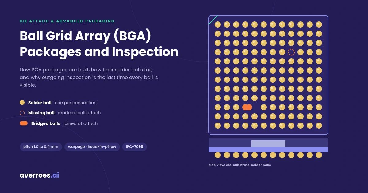
A ball grid array (BGA) is an IC package with a grid of solder balls on its underside instead of leads, used for high pin counts in a small footprint. The die sits on a substrate that routes signals to the balls. Because the balls hide their joints, BGA quality depends on ball attach, warpage and X-ray after reflow, and AI visual inspection platforms such as Averroes.ai help classify ball defects before packages ship.
BGA packaging sits in Stage 07 of the semiconductor manufacturing process. This guide follows a BGA from the packaging line to the board: how the package is built, how its balls are attached, what goes wrong, and where each problem can still be caught.
Key Notes
BGA replaces leads with a ball grid: the whole underside carries connections, at common pitches from 1.0 mm down to 0.4 mm.
Ball attach is a yield point: missing, joined and bridged balls start at the packaging line, before the board.
Warpage drives head-in-pillow: a 2015 OEM-EMS study named package warpage during reflow as the most significant contributor.
Joints hide once soldered: optics see the outer rows; X-ray and endoscopes reach the rest.
What Is a Ball Grid Array?
A ball grid array is a surface-mount IC package that carries its connections as a grid of solder balls on its underside, used for chips that need more connections than a perimeter of leads can provide. The BGA descends from the pin grid array, which covered one face of the package with pins; the BGA replaces those pins with balls that are reflowed directly onto the board, as Wikipedia’s entry describes.
A BGA package has four main parts. The silicon die is mounted on a substrate, usually organic laminate, ceramic or tape, which routes signals from the die to the solder balls. The solder balls connect to the printed circuit board. An encapsulant or lid protects the die. Lenovo’s technical glossary describes the same structure.
Because the whole underside carries connections, a BGA fits a high pin count into a small footprint. Common ball pitches are 1.0, 0.8, 0.65, 0.5 and 0.4 mm, according to the EmbeddedRelated glossary. BGA packaging is part of the die attach and advanced packaging stage of the hub.
What Are the Types of BGA Packages?
A BGA package type is a combination of how the die connects to the substrate and what the substrate is made of, used to match a package to its cost, pin count and thermal needs. Four types are common:
Plastic BGA (PBGA) mounts a die face up and connects it to an organic substrate by wire bonding, then encapsulates it in mold compound.
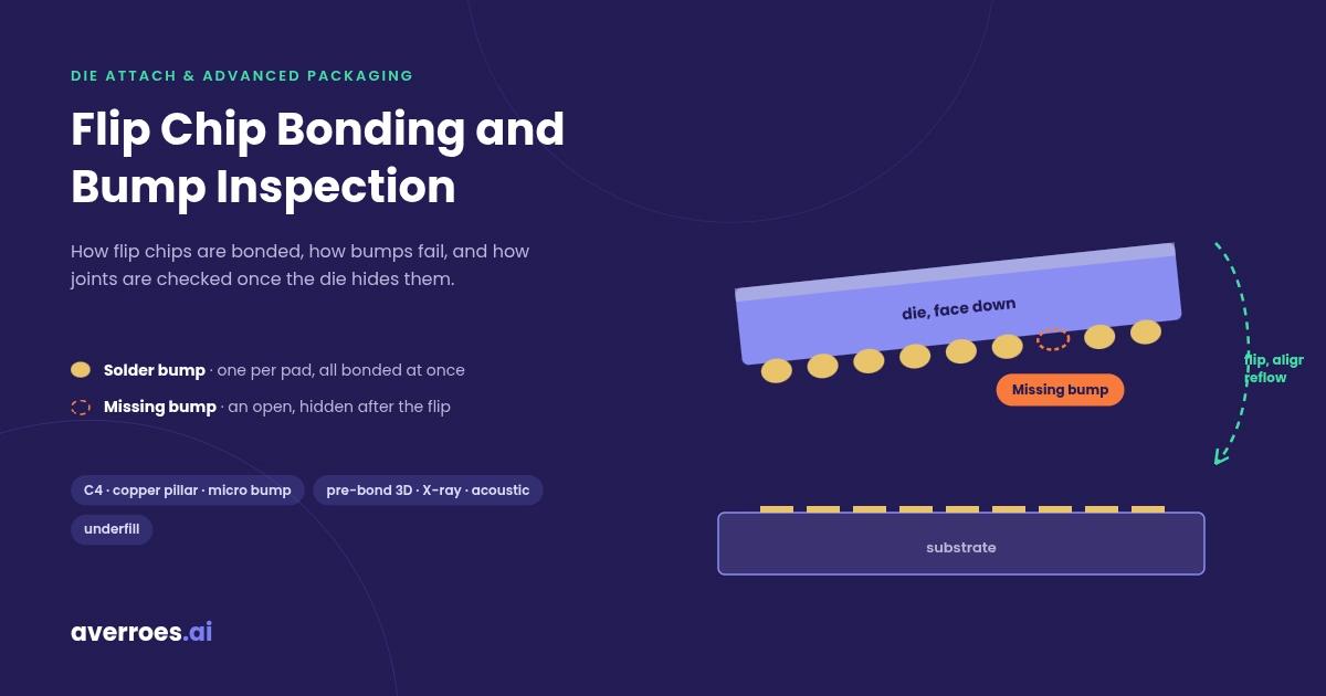
Flip chip BGA (FCBGA) mounts the die face down on the substrate through bumps, covered in flip chip bonding. It adds a second level of solder joints between die and substrate.
Ceramic BGA uses a ceramic substrate for thermal and reliability demands.
Package on package (PoP) stacks one BGA on another, with balls connecting the two packages.
The takeaway: every BGA type ends in the same place, a grid of solder balls that must all meet the board.
How Are Solder Balls Attached to a BGA Package?
Ball attach is the packaging step that places solder balls on the substrate’s pads and reflows them into place, used to give the package its board connections. In the common flux method, the pads are coated with flux, the balls are placed on them, and the package passes through a reflow oven where the balls melt onto the pads, as patent literature on ball placement describes.
Ball attach is a yield point in its own right. A study of ball attach materials by Jimarez and colleagues notes that pin transfer with tacky flux is the most popular method today, and that the process still suffers from missing balls, joined balls and bridging balls, which force rework. These are package defects, made before the BGA ever reaches a board.
Why Do BGA Packages Warp, and Why Does Coplanarity Matter?
Package warpage is the bending of the substrate out of flat, used as a key package specification because it moves the balls out of a single plane. Ball coplanarity is how closely the bottoms of all the balls match that plane.
A warped substrate leaves some balls higher than others. A patent filed in January 2007 on ball mounting explains the consequence: if warpage leaves the center balls lower than the edge balls, the edge balls contact the board while the center balls can lose contact, and the package fails. The same patent gives typical limits: coplanarity preferably under about 6 mils for substrates smaller than 37.5 by 37.5 mm, and under about 8 mils for larger ones. IPC-7095C, the industry guide for BGA design and assembly (January 2013), includes package and ball coplanarity among its BGA package acceptance criteria, alongside voids in solder balls and ball attach integrity. Warpage also shapes the metrology covered in advanced packaging metrology.
What Does BGA Underfill Do?
BGA underfill is an epoxy injected under a BGA after it is soldered to the board, used to glue the device to the board and spread mechanical and thermal stress across the joints, as Wikipedia’s entry describes. It is a board-level step, separate from the die-level underfill inside a flip chip package, which is covered in flip chip bonding. Underfill adds mechanical strength, but it also makes later rework far harder.
The takeaway: a BGA’s balls must be present, sound and coplanar before the package ever leaves the packaging line.
What Defects Affect BGA Packages and Solder Joints?
A BGA defect is a flaw in the balls, the package or the solder joints that causes an open, a short or a weak connection, used as the reject criteria at package outgoing and after board assembly. Some start at ball attach, and some appear only when the package is soldered to the board.
BGA defects and where they start
Defect
What It Is
Where It Starts
When It Can Be Caught
Missing ball
No ball on a pad
Ball attach
Package outgoing (optical)
Joined or bridged balls
Balls merged at attach
Ball attach
Package outgoing (optical)
Deformed or damaged ball
Ball out of shape
Ball attach, handling
Package outgoing (optical)
Coplanarity error
Balls out of one plane
Substrate warpage
Package outgoing (coplanarity measurement)
Oxidized or contaminated balls
Poor wetting surface
Storage, handling
Package outgoing, then at reflow
Voids
Gas pockets in a joint
Board reflow
After reflow (X-ray)
Bridging
Solder joining adjacent balls
Board reflow
After reflow (X-ray)
Head-in-pillow
Ball and paste melt but do not fuse
Board reflow, warpage
After reflow (X-ray, often hard)
Non-wet open
Ball not joined to the pad
Board reflow
After reflow (X-ray)
Sources: ball attach defects from Jimarez et al.; coplanarity from US patent 7642129 and IPC-7095C; board-level defects from SMT007 (July 2026) and Wikipedia.
The first five rows are package defects. The last four appear only at board assembly, but several of them trace back to the package: warpage and oxidized balls are two of the main causes of head-in-pillow.
What Is a Head-in-Pillow Defect?
A head-in-pillow defect is an incomplete solder joint in which the BGA ball and the solder paste both melt but do not merge, used as a name for one of the hardest BGA failures to catch. In cross-section, it looks like a head pressed into a soft pillow, as Mario Scalzo of Indium Corporation, a solder materials supplier, described it at IPC Electronics Midwest in 2010. He traced it to two main sources: poor wetting, from ball oxidation, an unsuitable reflow profile or weak flux, and warpage of the package or board.
Warpage is the larger factor. A 2015 collaboration between Alcatel-Lucent, Ericsson, Celestica, Flextronics, Sanmina and Plexus, published in SMT Magazine, named package warpage during reflow as the most significant contributor, and proposed a maximum warpage of 0.090 mm (3.5 mil) for BGAs of 0.8 mm pitch and above. A 2011 study in JOM used shadow moiré imaging to show packages warping more than 100 µm at the solder melting temperature, lifting balls out of the paste; as the assembly cools, the balls drop back onto paste that no longer wets.
The same 2015 study explains why head-in-pillow is dangerous: the close contact between ball and paste can escape X-ray inspection, and there is often enough electrical continuity to pass initial electrical test. The joint fails later, in the field.
The takeaway: some of the worst board-level BGA failures start as package problems.
How Are BGA Packages and Joints Inspected?
BGA inspection is a two-stage check, first of the balls on the finished package and then of the solder joints after board assembly, used because the joints become hidden once the package is soldered. Each stage sees what the other cannot.
Where BGA defects are caught
Stage
Method
What It Catches
Limit
Package outgoing
Optical ball inspection
Missing, joined, bridged, deformed or contaminated balls
Nothing about the board joint
Package outgoing
Coplanarity and warpage measurement
Balls out of plane, substrate warpage
Warpage changes at reflow temperature
After board reflow
Visual with microscope
Outer rows: wetting, alignment
Inner rows hidden
After board reflow
Endoscope
Some inner rows
Not every row
After board reflow
X-ray (2D, 3D or CT)
Voids, bridging, opens, many head-in-pillow joints
Marginal joints can escape
After board reflow
Electrical test and boundary scan
Connectivity
Marginal joints that pass now
At package outgoing, every ball is still visible, so optical inspection can check each one for presence, shape, bridging and contamination, and coplanarity can be measured against the package specification.
After board reflow, the joints sit under the package. A July 2026 SMT007 column on BGA inspection describes visual inspection with a microscope for the outer rows, endoscopes for some inner rows, and X-ray for internal joints, voids and bridging. It lists acceptance criteria from IPC-A-610 and J-STD-001, including voids of 30% or less of any ball and no head-in-pillow. X-ray methods are covered in automated X-ray inspection and X-ray inspection systems. The EmbeddedRelated glossary adds a limit: electrical test and boundary scan confirm connectivity but will not reveal a marginal joint that may fail later under thermal cycling.
Why Do Package-Side Defects Matter at the Board?
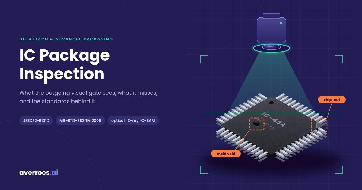
A package-side defect is a ball or coplanarity problem made at the packaging line, used here to explain why the outgoing gate matters so much. Once a BGA is soldered, its joints are hidden, and some of the defects that started at the package, such as head-in-pillow from warpage or oxidized balls, can escape X-ray and pass electrical test. Package outgoing inspection is the last point where every ball is fully visible. A defect that leaves the packaging line becomes the board assembler’s hidden failure. Board-level assembly and rework are covered in PCB visual inspection and PCB assembly inspection, and the package’s outer surface in IC package cosmetic inspection.
Catch Ball Defects Before They Reach the Board
Test AI defect classification on your own BGA ball images
The takeaway: inspect every ball before the package ships, because after reflow the board can only see some of the joints.
Where Does AI Fit in BGA Inspection?
AI BGA inspection is image-based classification that sorts ball and package images into specific defect classes and acceptable variation, used to inspect every ball at outgoing speed and to keep up as pitches and ball sizes change. A BGA carries hundreds or thousands of balls, and rule-based checks have to be retuned for every new pitch.
AI does four jobs in BGA inspection:
Classify ball defects on outgoing images, such as missing, joined, bridged, deformed or contaminated balls, and separate them from acceptable variation.
Adapt to new packages quickly, by training on a few labeled images of a new pitch or ball size instead of rewriting inspection rules.
Classify X-ray findings such as voids and bridging into defect classes for review, as a category capability on images the line already produces.
Trend defects by substrate lot and ball attach line, so a rise in missing or bridged balls points to the step behind it.
Averroes.ai runs AI defect classification on the images a packaging line already captures, using the same imaging approach described in die inspection. It trains from 20 to 40 labeled images per defect class, with no code, and deploys on premise. Averroes is not a warpage, X-ray or ball attach system: it works on the images those tools produce. You can test AI defect classification on your own BGA ball images.
Frequently Asked Questions
What is the difference between BGA and FCBGA?
A BGA is any package with solder balls on its underside. In a standard plastic BGA, the die sits face up and connects to the substrate with bond wires. In a flip chip BGA (FCBGA), the die sits face down and connects to the substrate through bumps, which adds a second level of hidden solder joints inside the package.
Why are BGA solder joints hard to inspect?
BGA solder joints sit between the package and the board, so once the package is soldered, optical inspection can see only the outer rows. Endoscopes reach some inner rows, and X-ray is used for internal joints, voids and bridging. Some defects, such as head-in-pillow, can still escape X-ray and pass electrical test.
What causes head-in-pillow defects in BGA?
Head-in-pillow defects form when the BGA ball and the solder paste both melt but do not merge. The main causes are package or board warpage during reflow, which lifts balls away from the paste, and poor wetting from oxidized balls, an unsuitable reflow profile or weak flux. A 2015 OEM-EMS study named warpage the most significant contributor.
What is BGA underfill?
BGA underfill is an epoxy injected under a BGA after it is soldered to the board. It glues the package to the board and spreads mechanical and thermal stress across the solder joints, improving reliability under shock, vibration and temperature cycling. It also makes later rework much harder.
What is BGA coplanarity?
BGA coplanarity is how closely the bottoms of all the solder balls match a single plane. Substrate warpage pushes some balls higher than others, so some may not reach the board at reflow. One patent gives preferred limits of about 6 mils for substrates under 37.5 mm and about 8 mils for larger ones.
What does IPC-7095 cover?
IPC-7095 is the industry guide for BGA design and assembly processes. Its C revision, published in January 2013, covers BGA package types, ball attach, board design, assembly and reliability, and includes package acceptance criteria for voids in solder balls, ball attach integrity, and package and ball coplanarity.






A ball grid array (BGA) is an IC package with a grid of solder balls on its underside instead of leads, used for high pin counts in a small footprint. The die sits on a substrate that routes signals to the balls. Because the balls hide their joints, BGA quality depends on ball attach, warpage and X-ray after reflow, and AI visual inspection platforms such as Averroes.ai help classify ball defects before packages ship.
BGA packaging sits in Stage 07 of the semiconductor manufacturing process. This guide follows a BGA from the packaging line to the board: how the package is built, how its balls are attached, what goes wrong, and where each problem can still be caught.
Key Notes
What Is a Ball Grid Array?
A ball grid array is a surface-mount IC package that carries its connections as a grid of solder balls on its underside, used for chips that need more connections than a perimeter of leads can provide. The BGA descends from the pin grid array, which covered one face of the package with pins; the BGA replaces those pins with balls that are reflowed directly onto the board, as Wikipedia’s entry describes.
A BGA package has four main parts. The silicon die is mounted on a substrate, usually organic laminate, ceramic or tape, which routes signals from the die to the solder balls. The solder balls connect to the printed circuit board. An encapsulant or lid protects the die. Lenovo’s technical glossary describes the same structure.
Because the whole underside carries connections, a BGA fits a high pin count into a small footprint. Common ball pitches are 1.0, 0.8, 0.65, 0.5 and 0.4 mm, according to the EmbeddedRelated glossary. BGA packaging is part of the die attach and advanced packaging stage of the hub.
What Are the Types of BGA Packages?
A BGA package type is a combination of how the die connects to the substrate and what the substrate is made of, used to match a package to its cost, pin count and thermal needs. Four types are common:
The takeaway: every BGA type ends in the same place, a grid of solder balls that must all meet the board.
How Are Solder Balls Attached to a BGA Package?
Ball attach is the packaging step that places solder balls on the substrate’s pads and reflows them into place, used to give the package its board connections. In the common flux method, the pads are coated with flux, the balls are placed on them, and the package passes through a reflow oven where the balls melt onto the pads, as patent literature on ball placement describes.
Ball attach is a yield point in its own right. A study of ball attach materials by Jimarez and colleagues notes that pin transfer with tacky flux is the most popular method today, and that the process still suffers from missing balls, joined balls and bridging balls, which force rework. These are package defects, made before the BGA ever reaches a board.
Why Do BGA Packages Warp, and Why Does Coplanarity Matter?
Package warpage is the bending of the substrate out of flat, used as a key package specification because it moves the balls out of a single plane. Ball coplanarity is how closely the bottoms of all the balls match that plane.
A warped substrate leaves some balls higher than others. A patent filed in January 2007 on ball mounting explains the consequence: if warpage leaves the center balls lower than the edge balls, the edge balls contact the board while the center balls can lose contact, and the package fails. The same patent gives typical limits: coplanarity preferably under about 6 mils for substrates smaller than 37.5 by 37.5 mm, and under about 8 mils for larger ones. IPC-7095C, the industry guide for BGA design and assembly (January 2013), includes package and ball coplanarity among its BGA package acceptance criteria, alongside voids in solder balls and ball attach integrity. Warpage also shapes the metrology covered in advanced packaging metrology.
What Does BGA Underfill Do?
BGA underfill is an epoxy injected under a BGA after it is soldered to the board, used to glue the device to the board and spread mechanical and thermal stress across the joints, as Wikipedia’s entry describes. It is a board-level step, separate from the die-level underfill inside a flip chip package, which is covered in flip chip bonding. Underfill adds mechanical strength, but it also makes later rework far harder.
The takeaway: a BGA’s balls must be present, sound and coplanar before the package ever leaves the packaging line.
What Defects Affect BGA Packages and Solder Joints?
A BGA defect is a flaw in the balls, the package or the solder joints that causes an open, a short or a weak connection, used as the reject criteria at package outgoing and after board assembly. Some start at ball attach, and some appear only when the package is soldered to the board.
BGA defects and where they start
Sources: ball attach defects from Jimarez et al.; coplanarity from US patent 7642129 and IPC-7095C; board-level defects from SMT007 (July 2026) and Wikipedia.
The first five rows are package defects. The last four appear only at board assembly, but several of them trace back to the package: warpage and oxidized balls are two of the main causes of head-in-pillow.
What Is a Head-in-Pillow Defect?
A head-in-pillow defect is an incomplete solder joint in which the BGA ball and the solder paste both melt but do not merge, used as a name for one of the hardest BGA failures to catch. In cross-section, it looks like a head pressed into a soft pillow, as Mario Scalzo of Indium Corporation, a solder materials supplier, described it at IPC Electronics Midwest in 2010. He traced it to two main sources: poor wetting, from ball oxidation, an unsuitable reflow profile or weak flux, and warpage of the package or board.
Warpage is the larger factor. A 2015 collaboration between Alcatel-Lucent, Ericsson, Celestica, Flextronics, Sanmina and Plexus, published in SMT Magazine, named package warpage during reflow as the most significant contributor, and proposed a maximum warpage of 0.090 mm (3.5 mil) for BGAs of 0.8 mm pitch and above. A 2011 study in JOM used shadow moiré imaging to show packages warping more than 100 µm at the solder melting temperature, lifting balls out of the paste; as the assembly cools, the balls drop back onto paste that no longer wets.
The same 2015 study explains why head-in-pillow is dangerous: the close contact between ball and paste can escape X-ray inspection, and there is often enough electrical continuity to pass initial electrical test. The joint fails later, in the field.
The takeaway: some of the worst board-level BGA failures start as package problems.
How Are BGA Packages and Joints Inspected?
BGA inspection is a two-stage check, first of the balls on the finished package and then of the solder joints after board assembly, used because the joints become hidden once the package is soldered. Each stage sees what the other cannot.
Where BGA defects are caught
At package outgoing, every ball is still visible, so optical inspection can check each one for presence, shape, bridging and contamination, and coplanarity can be measured against the package specification.
After board reflow, the joints sit under the package. A July 2026 SMT007 column on BGA inspection describes visual inspection with a microscope for the outer rows, endoscopes for some inner rows, and X-ray for internal joints, voids and bridging. It lists acceptance criteria from IPC-A-610 and J-STD-001, including voids of 30% or less of any ball and no head-in-pillow. X-ray methods are covered in automated X-ray inspection and X-ray inspection systems. The EmbeddedRelated glossary adds a limit: electrical test and boundary scan confirm connectivity but will not reveal a marginal joint that may fail later under thermal cycling.
Why Do Package-Side Defects Matter at the Board?
A package-side defect is a ball or coplanarity problem made at the packaging line, used here to explain why the outgoing gate matters so much. Once a BGA is soldered, its joints are hidden, and some of the defects that started at the package, such as head-in-pillow from warpage or oxidized balls, can escape X-ray and pass electrical test. Package outgoing inspection is the last point where every ball is fully visible. A defect that leaves the packaging line becomes the board assembler’s hidden failure. Board-level assembly and rework are covered in PCB visual inspection and PCB assembly inspection, and the package’s outer surface in IC package cosmetic inspection.
Catch Ball Defects Before They Reach the Board
Test AI defect classification on your own BGA ball images
The takeaway: inspect every ball before the package ships, because after reflow the board can only see some of the joints.
Where Does AI Fit in BGA Inspection?
AI BGA inspection is image-based classification that sorts ball and package images into specific defect classes and acceptable variation, used to inspect every ball at outgoing speed and to keep up as pitches and ball sizes change. A BGA carries hundreds or thousands of balls, and rule-based checks have to be retuned for every new pitch.
AI does four jobs in BGA inspection:
Averroes.ai runs AI defect classification on the images a packaging line already captures, using the same imaging approach described in die inspection. It trains from 20 to 40 labeled images per defect class, with no code, and deploys on premise. Averroes is not a warpage, X-ray or ball attach system: it works on the images those tools produce. You can test AI defect classification on your own BGA ball images.
Frequently Asked Questions
What is the difference between BGA and FCBGA?
A BGA is any package with solder balls on its underside. In a standard plastic BGA, the die sits face up and connects to the substrate with bond wires. In a flip chip BGA (FCBGA), the die sits face down and connects to the substrate through bumps, which adds a second level of hidden solder joints inside the package.
Why are BGA solder joints hard to inspect?
BGA solder joints sit between the package and the board, so once the package is soldered, optical inspection can see only the outer rows. Endoscopes reach some inner rows, and X-ray is used for internal joints, voids and bridging. Some defects, such as head-in-pillow, can still escape X-ray and pass electrical test.
What causes head-in-pillow defects in BGA?
Head-in-pillow defects form when the BGA ball and the solder paste both melt but do not merge. The main causes are package or board warpage during reflow, which lifts balls away from the paste, and poor wetting from oxidized balls, an unsuitable reflow profile or weak flux. A 2015 OEM-EMS study named warpage the most significant contributor.
What is BGA underfill?
BGA underfill is an epoxy injected under a BGA after it is soldered to the board. It glues the package to the board and spreads mechanical and thermal stress across the solder joints, improving reliability under shock, vibration and temperature cycling. It also makes later rework much harder.
What is BGA coplanarity?
BGA coplanarity is how closely the bottoms of all the solder balls match a single plane. Substrate warpage pushes some balls higher than others, so some may not reach the board at reflow. One patent gives preferred limits of about 6 mils for substrates under 37.5 mm and about 8 mils for larger ones.
What does IPC-7095 cover?
IPC-7095 is the industry guide for BGA design and assembly processes. Its C revision, published in January 2013, covers BGA package types, ball attach, board design, assembly and reliability, and includes package acceptance criteria for voids in solder balls, ball attach integrity, and package and ball coplanarity.