


The Latest Trends
Blog
Insights and stories change the industry of Semiconductor Defect Detection and Deep Learning

All Blogs
Semiconductor
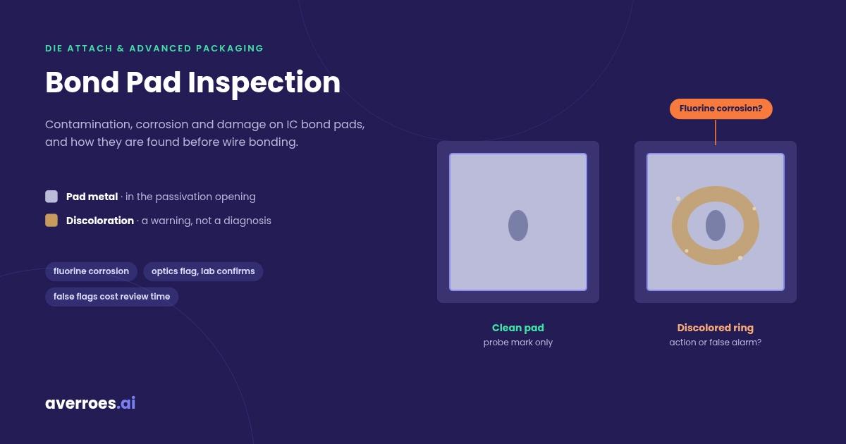
Bond Pad Inspection: How Contamination, Corrosion and Damage Are Found Before Wire Bonding
Learn more
Semiconductor
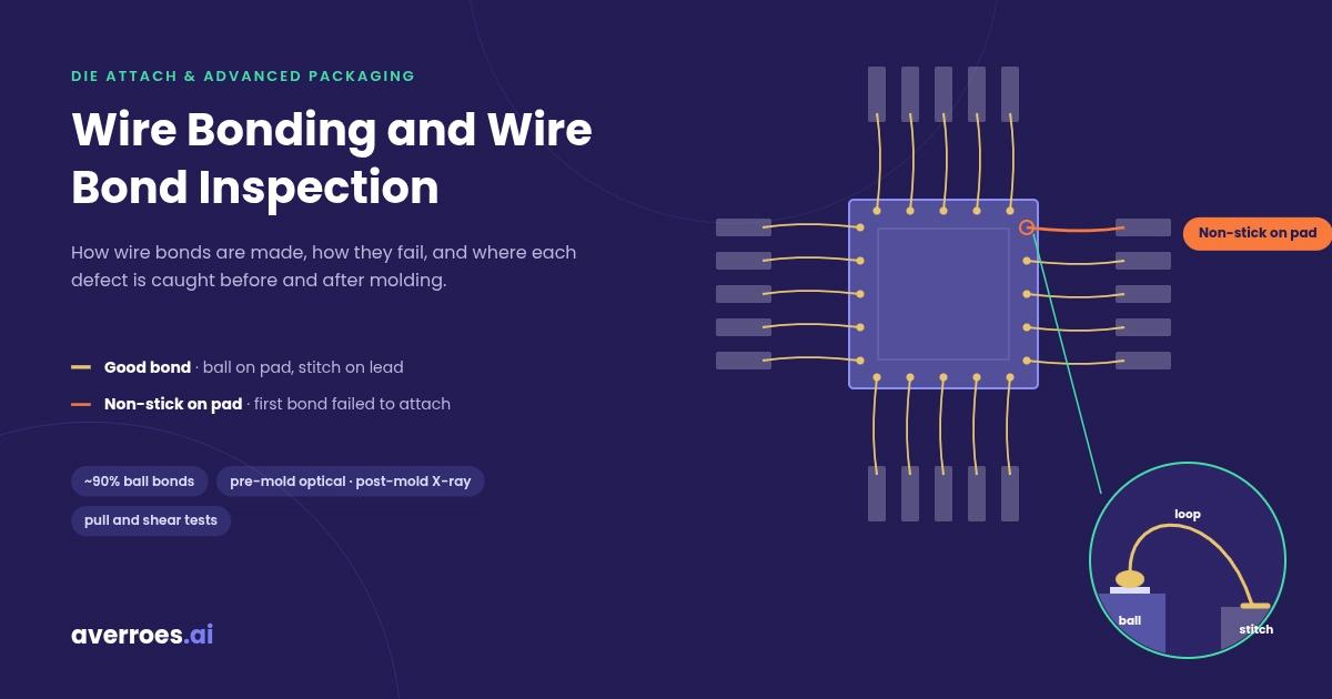
Wire Bonding: How Wire Bonds Are Made, How They Fail and How They Are Inspected
Learn more
Semiconductor
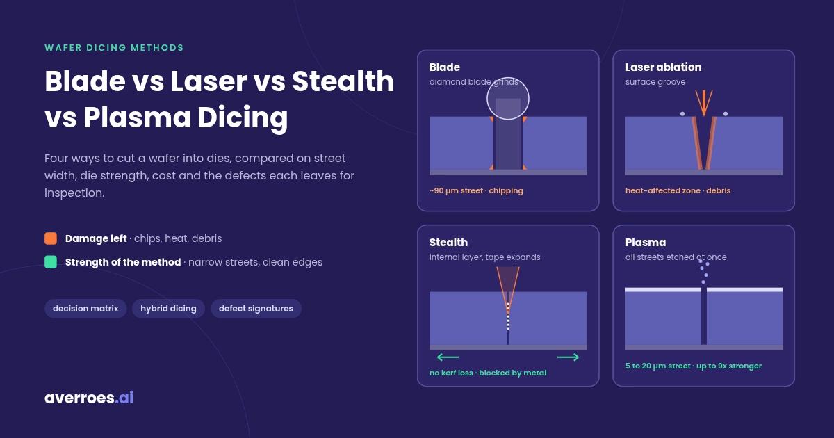
Wafer Dicing Methods Compared: Blade vs Laser vs Stealth vs Plasma Dicing
Learn more
Semiconductor
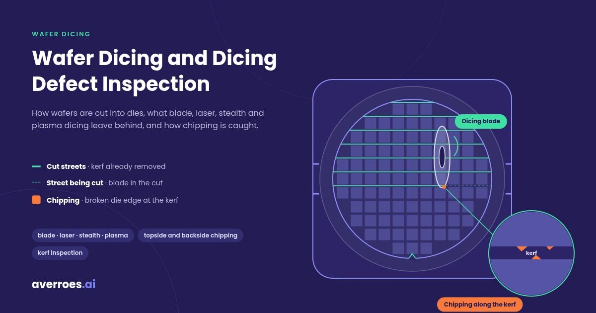
Wafer Dicing: How Wafers Are Cut Into Dies and How Dicing Defects Are Caught
Learn more
Semiconductor
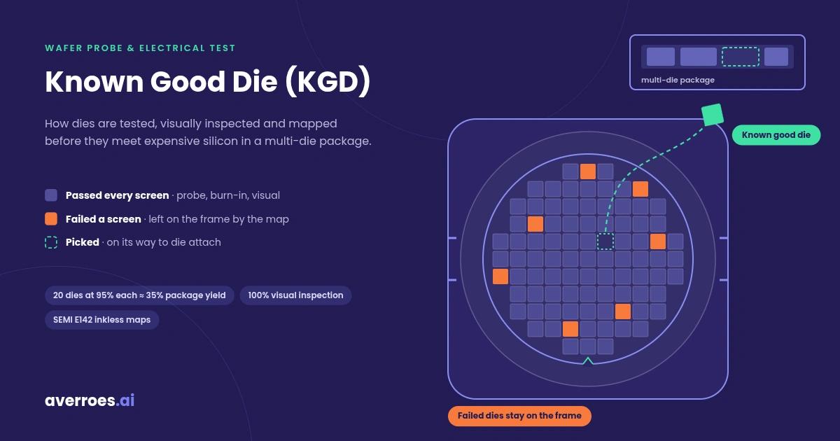
Known Good Die (KGD): How Dies Are Tested, Inspected and Mapped Before Packaging
Learn more
Semiconductor
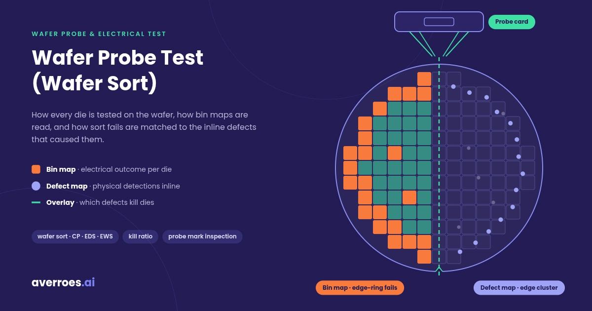
Wafer Probe Test (Wafer Sort): Bin Maps, Probe Marks and Defect Correlation
Learn more
Semiconductor
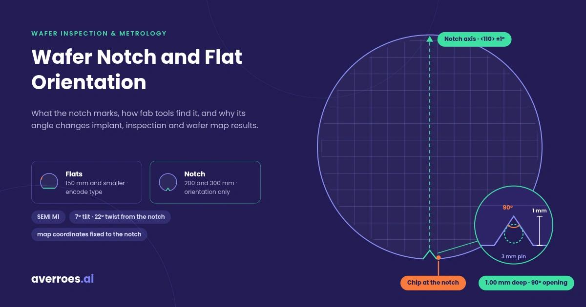
Wafer Notch and Flat: How Wafer Orientation Is Marked, Found and Inspected
Learn more

Semiconductor
Applied Materials Inspection Tools Explained: Enlight, SEMVision, PROVision and Where AI Fits
Learn more
Semiconductor
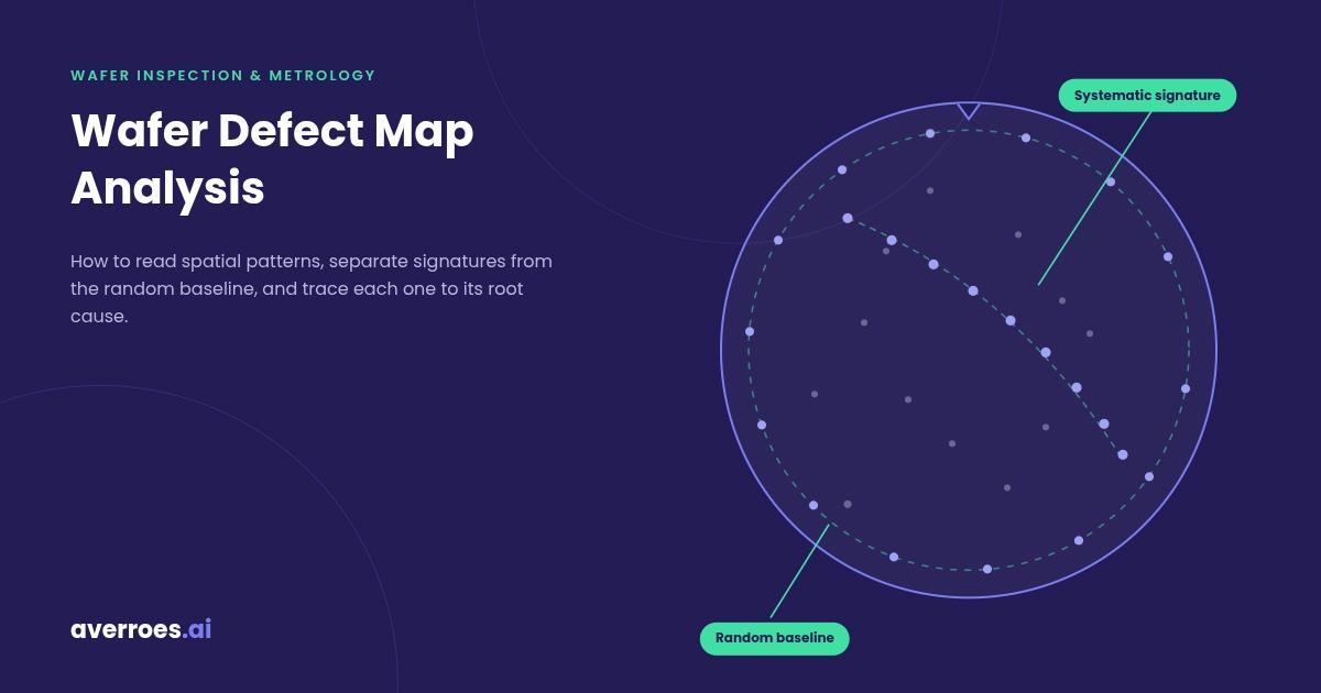
Wafer Defect Map Analysis: How to Read Spatial Patterns & Find Root Causes
Learn more

Experience the Averroes AI Advantage
Elevate Your Visual Inspection Capabilities
Request a Demo Now

Get Averroes AI's Monthly Newsletter
Stay updated with the latest news and resources delivered to your inbox.