Flip Chip Bonding: How Flip Chips Are Bonded, How Bumps Fail and How They Are Inspected
Averroes
Nov 17, 2026
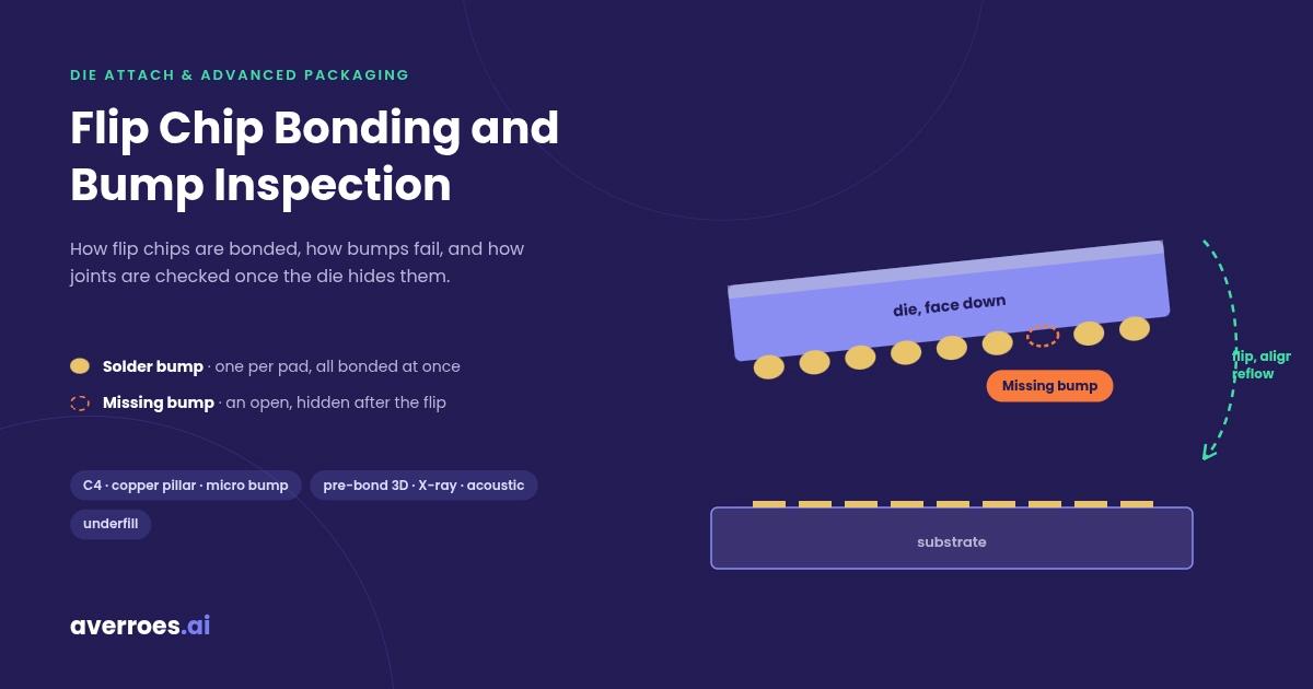
Flip chip bonding mounts a die face down on its substrate, connecting every pad at once through solder bumps or copper pillars instead of wires. Bumps are formed on the wafer, the dies are flipped, aligned and reflowed, and underfill fills the gap. Because the joints end up hidden, bumps are measured before bonding and checked by X-ray and acoustic imaging after, and AI visual inspection platforms such as Averroes.ai help segment bump defects.
Flip chip bonding sits in Stage 07 of the semiconductor manufacturing process, alongside wire bonding. This guide covers how flip chips are bonded, the bump types in use, the defects that matter, and how each one is caught before and after the joints disappear from view.
Key Notes
Flip chip is also called C4: IBM introduced it in 1964 and named it after the solder’s controlled collapse during reflow.
The whole chip surface can carry connections: bumps form an area array instead of a ring of wire pads at the edge.
Once flipped, every joint is hidden: optics measure bumps before bonding; X-ray and acoustic imaging check joints after.
Cured underfill blocks rework: catching bump defects before bonding is far cheaper than finding them after.
What Is Flip Chip Bonding?
Flip chip bonding is an interconnect method that mounts a die face down on its substrate through bumps on its pads, used to connect high-I/O and high-performance chips without wires. Flip chip, also known as controlled collapse chip connection or C4, connects a die to external circuitry with solder bumps deposited on the chip pads during the final wafer processing step, as Wikipedia’s flip chip entry describes.
The method is older than most of the chips that use it now. According to the Area Array Packaging Handbook, IBM first introduced flip chip in 1964 in the solid logic technology modules of its System/360 mainframe. The name comes from the solder bumps collapsing slightly during reflow, balancing the weight of the chip against the surface tension of the molten solder, which IBM controlled through solder volume and the wettable metal on chip and substrate.
What Is the Difference Between Flip Chip and Wire Bonding?
Flip chip and wire bonding are the two main ways to connect a die to its package: flip chip connects through bumps under the face-down die, used where I/O density and short connections matter, while wire bonding connects through fine wires from pads at the die edge, used for most cost-sensitive packages.
Flip chip vs wire bonding
Factor
Flip Chip Bonding
Wire Bonding
Connection
Solder bumps or copper pillars
Fine gold, copper or aluminum wire
Die orientation
Face down
Face up
Where connections sit
Area array across the die
Pads mostly around the edge
Connections made
All at once, at reflow
One wire at a time
Rework after underfill
Generally not possible
Not applicable
Inspection access
Joints hidden once flipped
Wires visible until molding
A 2005 Motorola patent on wafer-level packaging described C4’s advantages as substantial improvements in performance, size and I/O density, noted that virtually the entire chip surface can be used for pads, and reported over 2,500 C4 bumps demonstrated on a single chip. Those figures date from the patent; bump counts and pitches have moved far beyond them since.
How Does the Flip Chip Bonding Process Work?
The flip chip bonding process is a sequence of wafer-level and assembly steps that turns bumped dies into joined, underfilled packages, used to make every connection on a die in a single bonding step. It runs in 7 steps:
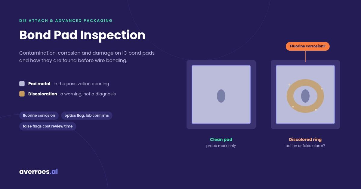
Prepare the pads. The die’s bond pads receive under bump metallization, a stack that gives the solder something to wet and adhere to. Pad condition matters here, as covered in bond pad inspection.
Bump the wafer. In wafer bumping, seed metal is sputtered onto the pads through a photoresist mask, the wafer is electroplated, the resist is stripped, and the solder is reflowed into its final bump shape.
Dice the wafer. The bumped wafer is cut into individual dies.
Flip and align. Each die is turned face down and aligned so its bumps sit on matching pads on the substrate.
Bond. The assembly is reflowed so the solder melts and joins. C4 reflow is largely self-aligning, as the solder’s wetting pulls the bumps onto their pads. Thermocompression bonding, which adds force and heat at the bond head, is used where warpage must be controlled.
Clean. Flux residue is removed, or a no-clean flux is used, so it does not interfere with underfill.
Underfill and cure. An epoxy underfill is dispensed into the gap between die and substrate and cured.
Sources: process steps and wafer bumping from Wikipedia’s flip chip entry and US patent 6103549; self-alignment from US patent 6953985; thermocompression use from Semiconductor Engineering (November 2025).
What Is the Difference Between C4 Solder Bumps and Copper Pillars?
A bump is the raised metal contact on a die pad that becomes the joint after bonding, used in several forms depending on pitch and application. Three types dominate:
C4 solder bumps are round solder bumps that collapse during reflow. Wikipedia gives typical solder ball diameters of 75 to 500 µm.
Copper pillar bumps are copper columns with a solder cap, soldered to substrate pads, as patent literature describes. The copper holds its shape during reflow, which allows finer pitch than a fully collapsing solder bump.
Micro bumps are small copper bumps used to stack dies in 2.5D and 3D packages. Semiconductor Engineering reported in November 2025 that HBM3E uses bumps of 30 to 20 µm and that HBM4 will likely scale to about 10 µm.
What Does Underfill Do?
Underfill is an epoxy fill between the die and the substrate, used to protect the solder joints from thermal stress. It distributes the thermal expansion mismatch between chip and substrate, preventing stress from concentrating in the joints and causing early failure, according to Wikipedia’s flip chip entry.
Underfill brings its own risk. Patent literature on flip chip defect detection notes that underfill is injected as a liquid, so air bubbles can become voids that cause localized heating and stress. Once cured, the underfill cannot be removed without damaging the chip, so an underfilled flip chip is generally not reworkable.
The takeaway: every connection is made at once, and after underfill there is no going back.
What Defects Affect Flip Chip Bumps and Joints?
A flip chip defect is a flaw in a bump, a joint or the underfill that causes an open, a short or a weak connection, used as the reject criteria before and after bonding. Some form during bumping, some at reflow and some during underfill.
Flip chip defects and where they come from
Defect
What It Is
Typical Cause
When It Can Be Caught
Missing bump
No bump on a pad
Bumping failure
Before bonding (optical); after (acoustic, X-ray)
Coplanarity error
Bumps of uneven height
Plating non-uniformity, process variation
Before bonding (3D optical)
Bridging
Solder joining adjacent bumps
Excess solder, tight pitch
After bonding (X-ray)
Solder voids
Gas pockets in a joint
Reflow, flux
After bonding (X-ray, acoustic)
Non-wet open
Solder not joined to the pad
Misalignment, die tilt, contamination
After bonding (X-ray)
Head-in-pillow
Bump resting on, not fused with, the pad solder
Misalignment, warpage
After bonding (X-ray)
Misalignment
Bumps off their pads
Placement, warpage
After bonding (X-ray)
Solder extrusion
Solder squeezed out of the joint
Excess solder, reflow profile
After bonding (X-ray)
Underfill voids and delamination
Gaps in or under the underfill
Trapped air, poor adhesion
After cure (acoustic)
Sources: Semiconductor Engineering, November 2025 (coplanarity, voids, non-wet, head-in-pillow, misalignment, extrusion); a published structural modal analysis paper and patent literature (missing bumps, bridging); US patent 7327448 and Ghaffarian, NASA JPL (underfill voids and delamination).
Head-in-pillow and non-wet defects are the hardest to manage because they can pass electrical test at first. Semiconductor Engineering described head-in-pillow as a latent defect that may show up only as a high-resistance connection, then fail completely as an open under later thermal or mechanical stress.
Why Does Bump Coplanarity Matter?
Bump coplanarity is the evenness of bump heights across a die, used as a pre-bond specification because every bump must touch its pad at reflow. Inconsistent bump height can come from plating non-uniformity and process variability, and the resulting misalignment causes opens and shorts during flip chip bonding, as Semiconductor Engineering reported in November 2025. Poor coplanarity also induces mechanical stress, interconnect fatigue and thermal cycling failures. The tighter the pitch, the less height variation the process can absorb.
The takeaway: the riskiest flip chip defects are the ones that pass test today and fail in the field.
How Are Flip Chip Bumps and Joints Inspected?
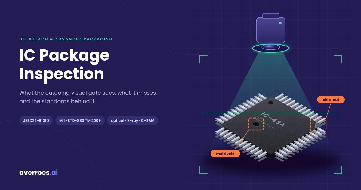
Flip chip inspection is the measurement of bumps before bonding and the non-destructive imaging of joints and underfill after it, used because the die hides every joint once it is flipped. Visual inspection, which works for wire bonds, is ineffective for bumps hidden under the chip, as patent literature on bump inspection notes.
Before bonding, the bumps are still visible. Semiconductor Engineering reported in November 2025 that IC makers typically focus on finding issues after plating and before reflow, and that automated optical inspection with laser triangulation measures bump height and coplanarity. Imaging methods for die-level optical inspection are covered in die inspection.
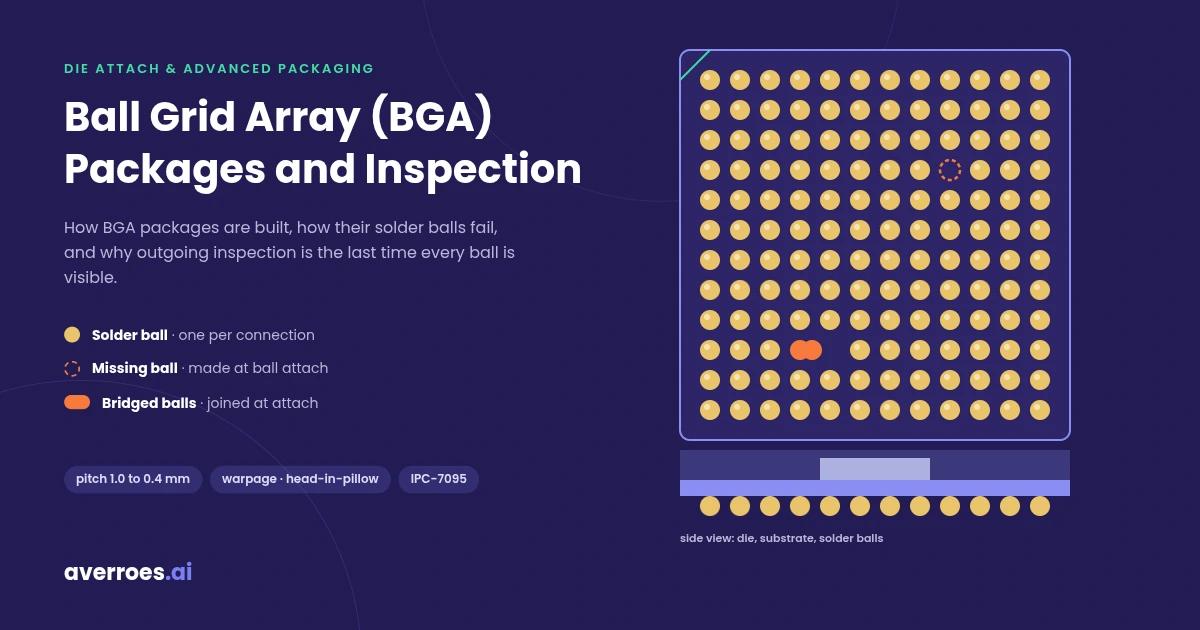
After bonding, X-ray sees through the die to the joints. X-ray methods are covered in automated X-ray inspection. Acoustic microscopy adds what X-ray misses: a NASA JPL paper by Reza Ghaffarian describes acoustic microscopy and X-ray as complementary non-destructive tools, with acoustic imaging suited to air-gap defects such as voids, delaminations and cracks in the underfill. Flip chips on ball grid array substrates (FCBGA) add a second level of solder joints, covered in BGA inspection.
Why Is Pre-Bond Bump Inspection Not Enough on Its Own?
Pre-bond bump inspection is the measurement of bumps on the wafer or die before flipping, used to stop bad bumps before they are hidden, but it cannot see what happens at reflow. Patent literature on bump inspection notes that some bump defects emerge only after reflow, so measuring bump dimensions before reflow alone can be misleading.
The post-bond tools have limits of their own. Acoustic imaging can take several minutes per chip, according to patent literature, which is too slow for every unit. And acoustic microscopy, the main way to find underfill voids, needs the part immersed in water and works only after the underfill has cured, when the part can no longer be reworked. Every defect caught before the flip is a package saved; every defect found after cure is a package lost.
Catch Bump Defects Before Underfill Locks Them In
Test AI defect segmentation on your own bump images
The takeaway: measure bumps before the flip, image joints after it, and expect each stage to miss what the other catches.
Where Does AI Fit in Flip Chip Inspection?
AI flip chip inspection is image-based segmentation and classification that outlines each bump and labels what is wrong with it, used to inspect thousands of bumps per die faster and more consistently than rules. Bumps are small, reflective and numerous, which makes rule-based measurement noisy as pitch shrinks.
Research shows the approach working. At IEEE ECTC 2025, A*STAR researchers presented a framework that segments each bump into copper pillar, copper pad, void and solder regions on 3D X-ray data, and reported a full report on more than 400 bumps in under 5 minutes, as Semiconductor Engineering summarized in November 2025. That is category evidence for AI segmentation, not an Averroes result.
AI does four jobs in flip chip inspection:
Segment bumps on pre-bond optical images and flag missing, deformed or bridged bumps on reflective surfaces.
Classify findings on X-ray and acoustic images, such as voids, non-wet joints and underfill gaps, into defect classes for review.
Trend defects by wafer, lot and bump layer, so a plating drift that hurts coplanarity shows up before bonding.
Feed die decisions, so only dies with good bumps move on as known good die into multi-die packages.
What is the difference between flip chip and wire bonding?
Flip chip bonding mounts the die face down and connects every pad at once through solder bumps or copper pillars, so connections can cover the whole die. Wire bonding mounts the die face up and connects pads one at a time with fine wires, mostly from the die edge. Flip chip joints are hidden after bonding; wire bonds stay visible until molding.
What does C4 mean in flip chip?
C4 stands for controlled collapse chip connection, IBM’s name for flip chip, introduced in 1964 for System/360 modules. The name describes the solder bumps collapsing slightly during reflow, balancing the chip’s weight against the solder’s surface tension. IBM controlled the collapse through solder volume and the wettable metal on chip and substrate.
What is underfill in flip chip packaging?
Underfill is an epoxy dispensed into the gap between a flip chip die and its substrate and then cured. It spreads the stress caused by different thermal expansion of chip and substrate, protecting the solder joints from early failure. Trapped air can leave voids, and cured underfill generally prevents rework.
What is a copper pillar bump?
A copper pillar bump is a copper column on a die pad topped with a solder cap, soldered to a pad on the substrate. Because the copper keeps its shape during reflow, copper pillars allow finer pitch than round C4 solder bumps, which collapse. They are common in high-density and advanced packages.
Why can’t flip chip joints be inspected optically after bonding?
Once a die is flipped face down, its bumps and joints sit between the die and the substrate, hidden from view. Optical inspection works only on bumps before bonding. After bonding, lines use X-ray to see through the die and scanning acoustic microscopy to find voids and delamination in the underfill.
What is bump coplanarity?
Bump coplanarity is how evenly the bumps on a die match in height. If some bumps are shorter, they may not touch their pads at reflow, causing opens, while misalignment can cause shorts. Uneven height can come from plating non-uniformity and process variation, so bump height is measured before bonding.






Flip chip bonding mounts a die face down on its substrate, connecting every pad at once through solder bumps or copper pillars instead of wires. Bumps are formed on the wafer, the dies are flipped, aligned and reflowed, and underfill fills the gap. Because the joints end up hidden, bumps are measured before bonding and checked by X-ray and acoustic imaging after, and AI visual inspection platforms such as Averroes.ai help segment bump defects.
Flip chip bonding sits in Stage 07 of the semiconductor manufacturing process, alongside wire bonding. This guide covers how flip chips are bonded, the bump types in use, the defects that matter, and how each one is caught before and after the joints disappear from view.
Key Notes
What Is Flip Chip Bonding?
Flip chip bonding is an interconnect method that mounts a die face down on its substrate through bumps on its pads, used to connect high-I/O and high-performance chips without wires. Flip chip, also known as controlled collapse chip connection or C4, connects a die to external circuitry with solder bumps deposited on the chip pads during the final wafer processing step, as Wikipedia’s flip chip entry describes.
The method is older than most of the chips that use it now. According to the Area Array Packaging Handbook, IBM first introduced flip chip in 1964 in the solid logic technology modules of its System/360 mainframe. The name comes from the solder bumps collapsing slightly during reflow, balancing the weight of the chip against the surface tension of the molten solder, which IBM controlled through solder volume and the wettable metal on chip and substrate.
Flip chip bonding is part of the die attach and advanced packaging stage, and it underpins the bumped interconnects in 2.5D and 3D packages covered in advanced packaging metrology.
What Is the Difference Between Flip Chip and Wire Bonding?
Flip chip and wire bonding are the two main ways to connect a die to its package: flip chip connects through bumps under the face-down die, used where I/O density and short connections matter, while wire bonding connects through fine wires from pads at the die edge, used for most cost-sensitive packages.
Flip chip vs wire bonding
A 2005 Motorola patent on wafer-level packaging described C4’s advantages as substantial improvements in performance, size and I/O density, noted that virtually the entire chip surface can be used for pads, and reported over 2,500 C4 bumps demonstrated on a single chip. Those figures date from the patent; bump counts and pitches have moved far beyond them since.
How Does the Flip Chip Bonding Process Work?
The flip chip bonding process is a sequence of wafer-level and assembly steps that turns bumped dies into joined, underfilled packages, used to make every connection on a die in a single bonding step. It runs in 7 steps:
Sources: process steps and wafer bumping from Wikipedia’s flip chip entry and US patent 6103549; self-alignment from US patent 6953985; thermocompression use from Semiconductor Engineering (November 2025).
What Is the Difference Between C4 Solder Bumps and Copper Pillars?
A bump is the raised metal contact on a die pad that becomes the joint after bonding, used in several forms depending on pitch and application. Three types dominate:
What Does Underfill Do?
Underfill is an epoxy fill between the die and the substrate, used to protect the solder joints from thermal stress. It distributes the thermal expansion mismatch between chip and substrate, preventing stress from concentrating in the joints and causing early failure, according to Wikipedia’s flip chip entry.
Underfill brings its own risk. Patent literature on flip chip defect detection notes that underfill is injected as a liquid, so air bubbles can become voids that cause localized heating and stress. Once cured, the underfill cannot be removed without damaging the chip, so an underfilled flip chip is generally not reworkable.
The takeaway: every connection is made at once, and after underfill there is no going back.
What Defects Affect Flip Chip Bumps and Joints?
A flip chip defect is a flaw in a bump, a joint or the underfill that causes an open, a short or a weak connection, used as the reject criteria before and after bonding. Some form during bumping, some at reflow and some during underfill.
Flip chip defects and where they come from
Sources: Semiconductor Engineering, November 2025 (coplanarity, voids, non-wet, head-in-pillow, misalignment, extrusion); a published structural modal analysis paper and patent literature (missing bumps, bridging); US patent 7327448 and Ghaffarian, NASA JPL (underfill voids and delamination).
Head-in-pillow and non-wet defects are the hardest to manage because they can pass electrical test at first. Semiconductor Engineering described head-in-pillow as a latent defect that may show up only as a high-resistance connection, then fail completely as an open under later thermal or mechanical stress.
Why Does Bump Coplanarity Matter?
Bump coplanarity is the evenness of bump heights across a die, used as a pre-bond specification because every bump must touch its pad at reflow. Inconsistent bump height can come from plating non-uniformity and process variability, and the resulting misalignment causes opens and shorts during flip chip bonding, as Semiconductor Engineering reported in November 2025. Poor coplanarity also induces mechanical stress, interconnect fatigue and thermal cycling failures. The tighter the pitch, the less height variation the process can absorb.
The takeaway: the riskiest flip chip defects are the ones that pass test today and fail in the field.
How Are Flip Chip Bumps and Joints Inspected?
Flip chip inspection is the measurement of bumps before bonding and the non-destructive imaging of joints and underfill after it, used because the die hides every joint once it is flipped. Visual inspection, which works for wire bonds, is ineffective for bumps hidden under the chip, as patent literature on bump inspection notes.
Where each flip chip defect is caught
Before bonding, the bumps are still visible. Semiconductor Engineering reported in November 2025 that IC makers typically focus on finding issues after plating and before reflow, and that automated optical inspection with laser triangulation measures bump height and coplanarity. Imaging methods for die-level optical inspection are covered in die inspection.
After bonding, X-ray sees through the die to the joints. X-ray methods are covered in automated X-ray inspection. Acoustic microscopy adds what X-ray misses: a NASA JPL paper by Reza Ghaffarian describes acoustic microscopy and X-ray as complementary non-destructive tools, with acoustic imaging suited to air-gap defects such as voids, delaminations and cracks in the underfill. Flip chips on ball grid array substrates (FCBGA) add a second level of solder joints, covered in BGA inspection.
Why Is Pre-Bond Bump Inspection Not Enough on Its Own?
Pre-bond bump inspection is the measurement of bumps on the wafer or die before flipping, used to stop bad bumps before they are hidden, but it cannot see what happens at reflow. Patent literature on bump inspection notes that some bump defects emerge only after reflow, so measuring bump dimensions before reflow alone can be misleading.
The post-bond tools have limits of their own. Acoustic imaging can take several minutes per chip, according to patent literature, which is too slow for every unit. And acoustic microscopy, the main way to find underfill voids, needs the part immersed in water and works only after the underfill has cured, when the part can no longer be reworked. Every defect caught before the flip is a package saved; every defect found after cure is a package lost.
Catch Bump Defects Before Underfill Locks Them In
Test AI defect segmentation on your own bump images
The takeaway: measure bumps before the flip, image joints after it, and expect each stage to miss what the other catches.
Where Does AI Fit in Flip Chip Inspection?
AI flip chip inspection is image-based segmentation and classification that outlines each bump and labels what is wrong with it, used to inspect thousands of bumps per die faster and more consistently than rules. Bumps are small, reflective and numerous, which makes rule-based measurement noisy as pitch shrinks.
Research shows the approach working. At IEEE ECTC 2025, A*STAR researchers presented a framework that segments each bump into copper pillar, copper pad, void and solder regions on 3D X-ray data, and reported a full report on more than 400 bumps in under 5 minutes, as Semiconductor Engineering summarized in November 2025. That is category evidence for AI segmentation, not an Averroes result.
AI does four jobs in flip chip inspection:
Averroes.ai runs AI defect segmentation and AI defect classification on the images a flip chip line already captures. It trains from 20 to 40 labeled images per defect class, with no code, and deploys on premise. Averroes is not a 3D metrology, X-ray or acoustic system: it works on the images those tools produce. You can test AI defect segmentation on your own bump images.
Frequently Asked Questions
What is the difference between flip chip and wire bonding?
Flip chip bonding mounts the die face down and connects every pad at once through solder bumps or copper pillars, so connections can cover the whole die. Wire bonding mounts the die face up and connects pads one at a time with fine wires, mostly from the die edge. Flip chip joints are hidden after bonding; wire bonds stay visible until molding.
What does C4 mean in flip chip?
C4 stands for controlled collapse chip connection, IBM’s name for flip chip, introduced in 1964 for System/360 modules. The name describes the solder bumps collapsing slightly during reflow, balancing the chip’s weight against the solder’s surface tension. IBM controlled the collapse through solder volume and the wettable metal on chip and substrate.
What is underfill in flip chip packaging?
Underfill is an epoxy dispensed into the gap between a flip chip die and its substrate and then cured. It spreads the stress caused by different thermal expansion of chip and substrate, protecting the solder joints from early failure. Trapped air can leave voids, and cured underfill generally prevents rework.
What is a copper pillar bump?
A copper pillar bump is a copper column on a die pad topped with a solder cap, soldered to a pad on the substrate. Because the copper keeps its shape during reflow, copper pillars allow finer pitch than round C4 solder bumps, which collapse. They are common in high-density and advanced packages.
Why can’t flip chip joints be inspected optically after bonding?
Once a die is flipped face down, its bumps and joints sit between the die and the substrate, hidden from view. Optical inspection works only on bumps before bonding. After bonding, lines use X-ray to see through the die and scanning acoustic microscopy to find voids and delamination in the underfill.
What is bump coplanarity?
Bump coplanarity is how evenly the bumps on a die match in height. If some bumps are shorter, they may not touch their pads at reflow, causing opens, while misalignment can cause shorts. Uneven height can come from plating non-uniformity and process variation, so bump height is measured before bonding.