Wafer Dicing Methods Compared: Blade vs Laser vs Stealth vs Plasma Dicing
Averroes
Nov 13, 2026
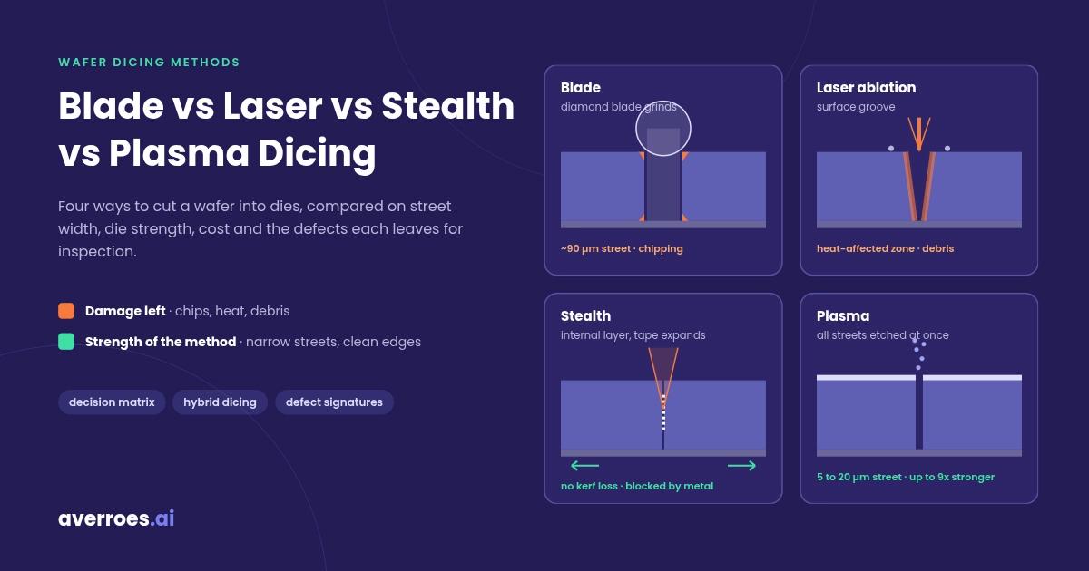
The four main wafer dicing methods are blade dicing, laser ablation, stealth dicing and plasma dicing. Blade dicing is the cheapest and most widely used but chips edges; laser ablation leaves heat damage; stealth dicing leaves almost no kerf but cannot cut through metal in the streets; plasma dicing gives narrow streets and much stronger dies than sawing. Each leaves a different defect signature, which AI visual inspection platforms such as Averroes.ai are trained to classify.
Dicing methods sit in Stage 06 of the semiconductor manufacturing process, and the dicing process itself is covered in wafer dicing. This guide compares the four methods side by side, explains where each falls short, and shows how the choice changes what post-dicing inspection has to find.
Key Notes
Plasma dicing makes the narrowest streets: 5 to 20 µm, against about 90 µm for a saw, in a 2015 ON Semiconductor and Plasma-Therm study.
Plasma-diced dies can be far stronger: up to 9 times the strength of sawn dies in the same study.
Stealth dicing cannot cut through metal: test structures and alignment marks in the street block the laser.
Low-k wafers usually need two steps: laser grooving removes the fragile layers, then a blade cuts the silicon.
What Are the Main Wafer Dicing Methods?
A wafer dicing method is the technique used to separate a processed wafer into individual dies, used to set how much silicon is lost, how strong the dies are and what damage inspection must look for. Four methods dominate, and they work in very different ways:
Blade dicing grinds through each street with a thin diamond blade.
Laser ablation dicing vaporizes a groove from the wafer surface.
Stealth dicing focuses a laser inside the wafer to create a weakened layer, then separates the dies by stretching the tape.
Plasma dicing etches every street away chemically, all at once.
Lines also combine them. Hybrid dicing pairs a laser step with a blade, or a dicing step with backgrinding, to handle wafers no single method cuts well.
“Laser dicing” is used loosely for two different methods. Ablation cuts from the surface and removes material; stealth dicing works inside the wafer and removes almost none. This guide treats them separately because their damage, limits and inspection needs are different. Older techniques such as scribe and break still exist but are outside the scope here. All of these methods belong to the wafer dicing stage of the hub.
How Do Blade, Laser, Stealth and Plasma Dicing Compare?
A dicing method comparison is a side-by-side view of how each method cuts and what it costs in silicon, strength and damage, used to narrow the choice before process trials. The table uses only sourced descriptions; where no source reports a value, it says so.
Wafer dicing methods compared
Factor
Blade Dicing
Laser Ablation
Stealth Dicing
Plasma Dicing
How it cuts
Diamond blade grinds the street
Laser vaporizes a surface groove
Internal laser layer, tape expansion
Fluorine plasma etches all streets
Street width
About 90 µm saw street
Not reported
No kerf loss (maker’s claim)
5 to 20 µm
Die strength
Reduced by chipping
Weakened by heat-affected zone
No top or bottom chipping (maker’s claim)
Up to 9 times sawn dies
Heat or debris
Debris, cooling-water stress
Heat damage, molten debris
Not reported
No mechanical or heat damage
Metal or low-k in street
Low-k peels; usually laser-grooved first
Used to groove low-k and copper
Metal blocks the laser
Streets defined by masking
Relative cost
Lowest; most widely used
Considerably above blade
Not reported
Can lower cost as dies shrink (supplier view)
Defect signature for inspection
Chips, cracks, kerf drift
Debris, heat marks, microcracks
Crack-path errors, delamination
Backside notching, masking errors
Sources: street widths and die strength from Westerman et al. (ON Semiconductor, Plasma-Therm), 228th ECS Meeting, October 2015; blade, laser and plasma behavior and costs from Barnett (KLA), August 2022, and Hamamatsu; stealth limits from patent literature. Hamamatsu developed stealth dicing and KLA supplies plasma dicing, so their claims are labeled.
Every method leaves a different defect signature, and an inspection recipe tuned for one can miss the others.
Every Dicing Method Leaves a Signature
Test AI defect detection on images from your dicing line
The takeaway: no method wins on every row, so the choice depends on which rows matter for the product.
How Does Each Dicing Method Work, and Where Does It Fall Short?
Each dicing method is a different way of separating dies, and each has a characteristic failure mode, used to decide where it fits and what to inspect for after it runs.
How Does Blade Dicing Work?
Blade dicing is a mechanical method that grinds through each street with a thin, high-speed diamond wheel, used as the default singulation process across the industry. Wevolver’s 2023 guide describes it as the most widely used method, and it remains the reference point the others are measured against.
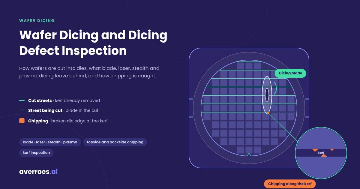
Its weakness is that it removes material by force. KLA’s August 2022 overview notes that physical removal can chip and crack the die. Hamamatsu, which developed stealth dicing, lists further problems: stress and recontamination from vibration and cooling water, and scattered debris that can damage fragile structures. Blade dicing also struggles when the street holds materials the blade cuts badly, such as low-k dielectric and copper. Chips and cracks from blade dicing are the main targets of crack inspection after dicing.
How Does Laser Ablation Dicing Work?
Laser ablation dicing is a thermal method that focuses a laser on the wafer surface and vaporizes a groove through the street, used where a blade would damage the surface layers or as the first step of a hybrid process. Laser wafer dicing removes material without mechanical contact, so it avoids vibration damage.
Heat is its cost. Ablation leaves a heat-affected zone that weakens the die, plus molten debris and microcracks along the cut, as a Photonics.com article on dicing technologies describes. KLA’s 2022 overview adds that laser dicing is considerably more costly than blade dicing. In practice, ablation is most often used for laser grooving: removing the fragile top layers before a blade finishes the cut.
How Does Stealth Dicing Work?
Stealth dicing is a laser method that focuses a beam at a wavelength silicon transmits inside the wafer, creating a modified layer, and then separates the dies by expanding the tape, used for clean, kerf-free separation of silicon wafers. Hamamatsu, which developed the method, describes it as having no kerf loss and no chipping on the top and bottom surfaces of the chip.
Its limits come from that internal approach. Patent literature, including an Applied Materials hybrid dicing patent, notes that the stealth laser cannot penetrate metal layers in the street, such as alignment marks and test element groups (TEGs), so lines have to irradiate from the backside instead. The same patent family describes weak control over how the induced cracks propagate, which can cause metal peeling and dielectric delamination. A University of Iowa preprint on low-k dicing states that stealth dicing is ineffective for opaque or heavily doped wafers and cannot be applied to devices with low-k layers. That source is a preprint, not yet peer reviewed.
How Does Plasma Dicing Work, and When Is It Worth It?
Plasma dicing is a dry-etch method that removes the street material with a fluorine plasma, etching every street on the wafer at the same time, used for thin, small or fragile dies where mechanical and thermal damage are not acceptable. KLA’s 2022 overview describes it as causing no mechanical damage and no heat-affected zone, with only gaseous by-products that are pumped away.
The numbers behind it are striking. A 2015 paper by ON Semiconductor and Plasma-Therm at the 228th ECS Meeting compared saw streets of about 90 µm with plasma dicing streets of 5 to 20 µm, and reported plasma-diced dies up to 9 times stronger than mechanically sawed dies. Narrower streets mean more dies per wafer, and the gain grows as dies get smaller.
Throughput works differently too. Blade and laser dicing are serial: they cut one street after another. Plasma dicing is parallel, so its time per wafer barely changes with the number of streets. The ECS paper describes it as supporting the trend to wafers of 50 µm and thinner. KLA adds that plasma dicing frees designers from straight dicing lanes, allowing non-rectangular dies and better use of wafer area.
Plasma dicing is most worth it in four cases:
Very thin wafers, where mechanical dicing damage grows and industry roadmaps push die thickness below 50 µm.
Small dies, where narrow streets add the most dies per wafer.
Stacked dies, such as hybrid-bonded high bandwidth memory, where one cracked die loses the whole stack and particles must be avoided. The same pressures shape advanced packaging metrology.
Fragile devices such as MEMS, where vibration and particles can damage moving structures.
Plasma dicing has its own process demands. The ECS paper names maintaining tape integrity and defining the streets with masks as integration issues, and patent literature describes backside notching at the tape interface as a defect that newer plasma processes are designed to avoid.
What Is Hybrid Dicing, and When Is It Used?
Hybrid dicing is a combination of two dicing steps, or of dicing and backgrinding, used for wafers that no single method separates cleanly. Three combinations cover most cases.
Laser grooving, then blade. When low-k dielectric or copper sits in the street, DISCO’s application notes state that blade dicing is usually performed after laser grooving. The laser removes the fragile wiring layers, and the blade cuts the silicon beneath. A March 2022 DISCO technical review describes the same sequence for low-k devices. Laser grooving is the standard answer to low-k peeling under a blade.
Backside stealth for metal streets. Because the stealth laser cannot pass through metal test structures in the street, patent literature describes irradiating the wafer from the backside instead, and some hybrids add a shallow blade groove on the front to guide the cracks.
Dicing before grinding. In dicing before grinding (DBG), the dies are defined by a partial cut from the front, then the wafer is ground from the back until the dies separate. A 2016 DISCO technical review reports that DBG greatly reduces backside chipping. The stealth version, stealth dicing before grinding (SDBG), gives narrow streets and higher die strength for thin dies, according to DISCO.
These combinations have limits of their own. An IMAPS paper on thin wafer dicing notes that very thin wafers with ultra low-k layers can break between laser grooving and blade dicing, and that stealth-before-grind struggles to reach yield as test structures thicken and wafers drop below 50 µm.
The takeaway: hybrid dicing exists because each single method has a material it cannot handle.
How Do You Choose a Wafer Dicing Method?
Choosing a wafer dicing method is a trade-off between wafer properties, street contents, die requirements and cost, used to pick the method or hybrid to qualify first. Six questions narrow it down:
How thin is the wafer? Backside chipping from blade dicing tends to increase as wafers get thinner, according to DISCO. Dicing before grinding, stealth before grinding or plasma dicing are the usual options for thin wafers, with plasma supporting 50 µm and below in the ECS study.
Is there low-k dielectric or copper in the street? Laser grooving followed by a blade is the standard route. Stealth dicing is not suited to low-k layers, per the University of Iowa preprint.
Is there metal in the street? Test structures and alignment marks block a stealth laser from the front, so stealth dicing needs backside irradiation or a different method.
How small are the dies, and how many fit on the wafer? Street width matters most for small dies. Plasma’s 5 to 20 µm streets and stealth dicing’s minimal kerf free the most area.
How strong must the dies be? For stacked dies and multi-die packages, die strength decides yield. Plasma-diced dies reached up to 9 times the strength of sawn dies in the ECS study, which matters wherever one cracked die scraps a known good die assembly.
What is the cost limit? Blade dicing remains the lowest-cost option, and KLA notes laser dicing is considerably more costly. Plasma can lower cost of ownership as dies shrink, by KLA’s account as a plasma dicing supplier.
The takeaway: start from the wafer and the street, then let die size, strength and cost decide between the remaining options.
How Does the Dicing Method Change Inspection?
Post-dicing inspection is the check of every die edge, sidewall and kerf for damage, used to stop damaged dies before die pick, and the dicing method decides which damage it has to find. An inspection recipe tuned for one method’s defects can miss another’s.
Each method shifts what inspection should look for:
Blade dicing: topside and backside chips, cracks, and kerf drift as the blade wears.
Laser ablation: debris on the surface, heat discoloration at the edges and microcracks along the cut.
Stealth dicing: cracks that wander from the intended path, metal peeling and dielectric delamination.
Plasma dicing: backside notching at the tape interface and errors where the street mask was defined.
The defects themselves are covered in dicing defects, and how die images are captured and processed in die inspection.
Changing dicing method, or running two methods on different products, means the inspection model has to learn new defect classes. Averroes.ai runs AI defect detection and AI defect classification on the kerf and post-dicing images a line already captures, trains from 20 to 40 labeled images per defect class with no code, and deploys on premise. That makes retraining for a new method’s signature a matter of labeling a few dozen images, not rewriting rules. Averroes does not sell or recommend dicing equipment: it works on the images the line produces. You can test AI defect detection on images from your dicing line.
Frequently Asked Questions
What is the difference between stealth dicing and laser dicing?
Laser ablation dicing focuses a laser on the wafer surface and vaporizes a groove, which removes material and leaves heat damage and debris. Stealth dicing focuses the laser inside the wafer to form a weakened layer, then separates dies by stretching the tape, with no kerf loss. Stealth dicing cannot cut through metal in the street.
Is plasma dicing better than blade dicing?
Plasma dicing gives narrower streets and stronger dies: a 2015 ECS study reported 5 to 20 µm streets against about 90 µm for a saw, and dies up to 9 times stronger. Blade dicing remains cheaper and more widely used, so plasma is usually chosen for thin, small, stacked or fragile dies.
Which dicing method is best for thin wafers?
Thin wafers suffer more backside chipping under a blade. The usual options are dicing before grinding, stealth dicing before grinding or plasma dicing, which an ECS study described as supporting wafers of 50 µm and thinner. The right choice also depends on what sits in the dicing streets.
Why is blade dicing still the most common method?
Blade dicing is the lowest-cost method, works on a wide range of wafers and is the established standard on most lines. Laser dicing costs considerably more, according to KLA, and plasma dicing needs masking and process changes. For standard-thickness wafers without fragile layers, a blade remains good enough.
What is laser grooving?
Laser grooving is a laser ablation step that removes the fragile top layers, such as low-k dielectric and copper, from the dicing street before a blade cuts the silicon underneath. It prevents the peeling and chipping a blade causes in those layers, and is the standard first step for low-k wafers.
Can stealth dicing cut wafers with metal in the streets?
Not from the front. The stealth dicing laser cannot pass through metal layers such as test structures and alignment marks in the street. Lines either irradiate the wafer from the backside, through the silicon, or remove the metal first, or choose a different dicing method.






The four main wafer dicing methods are blade dicing, laser ablation, stealth dicing and plasma dicing. Blade dicing is the cheapest and most widely used but chips edges; laser ablation leaves heat damage; stealth dicing leaves almost no kerf but cannot cut through metal in the streets; plasma dicing gives narrow streets and much stronger dies than sawing. Each leaves a different defect signature, which AI visual inspection platforms such as Averroes.ai are trained to classify.
Dicing methods sit in Stage 06 of the semiconductor manufacturing process, and the dicing process itself is covered in wafer dicing. This guide compares the four methods side by side, explains where each falls short, and shows how the choice changes what post-dicing inspection has to find.
Key Notes
What Are the Main Wafer Dicing Methods?
A wafer dicing method is the technique used to separate a processed wafer into individual dies, used to set how much silicon is lost, how strong the dies are and what damage inspection must look for. Four methods dominate, and they work in very different ways:
Lines also combine them. Hybrid dicing pairs a laser step with a blade, or a dicing step with backgrinding, to handle wafers no single method cuts well.
“Laser dicing” is used loosely for two different methods. Ablation cuts from the surface and removes material; stealth dicing works inside the wafer and removes almost none. This guide treats them separately because their damage, limits and inspection needs are different. Older techniques such as scribe and break still exist but are outside the scope here. All of these methods belong to the wafer dicing stage of the hub.
How Do Blade, Laser, Stealth and Plasma Dicing Compare?
A dicing method comparison is a side-by-side view of how each method cuts and what it costs in silicon, strength and damage, used to narrow the choice before process trials. The table uses only sourced descriptions; where no source reports a value, it says so.
Wafer dicing methods compared
Sources: street widths and die strength from Westerman et al. (ON Semiconductor, Plasma-Therm), 228th ECS Meeting, October 2015; blade, laser and plasma behavior and costs from Barnett (KLA), August 2022, and Hamamatsu; stealth limits from patent literature. Hamamatsu developed stealth dicing and KLA supplies plasma dicing, so their claims are labeled.
Every method leaves a different defect signature, and an inspection recipe tuned for one can miss the others.
Every Dicing Method Leaves a Signature
Test AI defect detection on images from your dicing line
The takeaway: no method wins on every row, so the choice depends on which rows matter for the product.
How Does Each Dicing Method Work, and Where Does It Fall Short?
Each dicing method is a different way of separating dies, and each has a characteristic failure mode, used to decide where it fits and what to inspect for after it runs.
How Does Blade Dicing Work?
Blade dicing is a mechanical method that grinds through each street with a thin, high-speed diamond wheel, used as the default singulation process across the industry. Wevolver’s 2023 guide describes it as the most widely used method, and it remains the reference point the others are measured against.
Its weakness is that it removes material by force. KLA’s August 2022 overview notes that physical removal can chip and crack the die. Hamamatsu, which developed stealth dicing, lists further problems: stress and recontamination from vibration and cooling water, and scattered debris that can damage fragile structures. Blade dicing also struggles when the street holds materials the blade cuts badly, such as low-k dielectric and copper. Chips and cracks from blade dicing are the main targets of crack inspection after dicing.
How Does Laser Ablation Dicing Work?
Laser ablation dicing is a thermal method that focuses a laser on the wafer surface and vaporizes a groove through the street, used where a blade would damage the surface layers or as the first step of a hybrid process. Laser wafer dicing removes material without mechanical contact, so it avoids vibration damage.
Heat is its cost. Ablation leaves a heat-affected zone that weakens the die, plus molten debris and microcracks along the cut, as a Photonics.com article on dicing technologies describes. KLA’s 2022 overview adds that laser dicing is considerably more costly than blade dicing. In practice, ablation is most often used for laser grooving: removing the fragile top layers before a blade finishes the cut.
How Does Stealth Dicing Work?
Stealth dicing is a laser method that focuses a beam at a wavelength silicon transmits inside the wafer, creating a modified layer, and then separates the dies by expanding the tape, used for clean, kerf-free separation of silicon wafers. Hamamatsu, which developed the method, describes it as having no kerf loss and no chipping on the top and bottom surfaces of the chip.
Its limits come from that internal approach. Patent literature, including an Applied Materials hybrid dicing patent, notes that the stealth laser cannot penetrate metal layers in the street, such as alignment marks and test element groups (TEGs), so lines have to irradiate from the backside instead. The same patent family describes weak control over how the induced cracks propagate, which can cause metal peeling and dielectric delamination. A University of Iowa preprint on low-k dicing states that stealth dicing is ineffective for opaque or heavily doped wafers and cannot be applied to devices with low-k layers. That source is a preprint, not yet peer reviewed.
How Does Plasma Dicing Work, and When Is It Worth It?
Plasma dicing is a dry-etch method that removes the street material with a fluorine plasma, etching every street on the wafer at the same time, used for thin, small or fragile dies where mechanical and thermal damage are not acceptable. KLA’s 2022 overview describes it as causing no mechanical damage and no heat-affected zone, with only gaseous by-products that are pumped away.
The numbers behind it are striking. A 2015 paper by ON Semiconductor and Plasma-Therm at the 228th ECS Meeting compared saw streets of about 90 µm with plasma dicing streets of 5 to 20 µm, and reported plasma-diced dies up to 9 times stronger than mechanically sawed dies. Narrower streets mean more dies per wafer, and the gain grows as dies get smaller.
Throughput works differently too. Blade and laser dicing are serial: they cut one street after another. Plasma dicing is parallel, so its time per wafer barely changes with the number of streets. The ECS paper describes it as supporting the trend to wafers of 50 µm and thinner. KLA adds that plasma dicing frees designers from straight dicing lanes, allowing non-rectangular dies and better use of wafer area.
Plasma dicing is most worth it in four cases:
Plasma dicing has its own process demands. The ECS paper names maintaining tape integrity and defining the streets with masks as integration issues, and patent literature describes backside notching at the tape interface as a defect that newer plasma processes are designed to avoid.
What Is Hybrid Dicing, and When Is It Used?
Hybrid dicing is a combination of two dicing steps, or of dicing and backgrinding, used for wafers that no single method separates cleanly. Three combinations cover most cases.
Laser grooving, then blade. When low-k dielectric or copper sits in the street, DISCO’s application notes state that blade dicing is usually performed after laser grooving. The laser removes the fragile wiring layers, and the blade cuts the silicon beneath. A March 2022 DISCO technical review describes the same sequence for low-k devices. Laser grooving is the standard answer to low-k peeling under a blade.
Backside stealth for metal streets. Because the stealth laser cannot pass through metal test structures in the street, patent literature describes irradiating the wafer from the backside instead, and some hybrids add a shallow blade groove on the front to guide the cracks.
Dicing before grinding. In dicing before grinding (DBG), the dies are defined by a partial cut from the front, then the wafer is ground from the back until the dies separate. A 2016 DISCO technical review reports that DBG greatly reduces backside chipping. The stealth version, stealth dicing before grinding (SDBG), gives narrow streets and higher die strength for thin dies, according to DISCO.
These combinations have limits of their own. An IMAPS paper on thin wafer dicing notes that very thin wafers with ultra low-k layers can break between laser grooving and blade dicing, and that stealth-before-grind struggles to reach yield as test structures thicken and wafers drop below 50 µm.
The takeaway: hybrid dicing exists because each single method has a material it cannot handle.
How Do You Choose a Wafer Dicing Method?
Choosing a wafer dicing method is a trade-off between wafer properties, street contents, die requirements and cost, used to pick the method or hybrid to qualify first. Six questions narrow it down:
The takeaway: start from the wafer and the street, then let die size, strength and cost decide between the remaining options.
How Does the Dicing Method Change Inspection?
Post-dicing inspection is the check of every die edge, sidewall and kerf for damage, used to stop damaged dies before die pick, and the dicing method decides which damage it has to find. An inspection recipe tuned for one method’s defects can miss another’s.
Each method shifts what inspection should look for:
The defects themselves are covered in dicing defects, and how die images are captured and processed in die inspection.
Changing dicing method, or running two methods on different products, means the inspection model has to learn new defect classes. Averroes.ai runs AI defect detection and AI defect classification on the kerf and post-dicing images a line already captures, trains from 20 to 40 labeled images per defect class with no code, and deploys on premise. That makes retraining for a new method’s signature a matter of labeling a few dozen images, not rewriting rules. Averroes does not sell or recommend dicing equipment: it works on the images the line produces. You can test AI defect detection on images from your dicing line.
Frequently Asked Questions
What is the difference between stealth dicing and laser dicing?
Laser ablation dicing focuses a laser on the wafer surface and vaporizes a groove, which removes material and leaves heat damage and debris. Stealth dicing focuses the laser inside the wafer to form a weakened layer, then separates dies by stretching the tape, with no kerf loss. Stealth dicing cannot cut through metal in the street.
Is plasma dicing better than blade dicing?
Plasma dicing gives narrower streets and stronger dies: a 2015 ECS study reported 5 to 20 µm streets against about 90 µm for a saw, and dies up to 9 times stronger. Blade dicing remains cheaper and more widely used, so plasma is usually chosen for thin, small, stacked or fragile dies.
Which dicing method is best for thin wafers?
Thin wafers suffer more backside chipping under a blade. The usual options are dicing before grinding, stealth dicing before grinding or plasma dicing, which an ECS study described as supporting wafers of 50 µm and thinner. The right choice also depends on what sits in the dicing streets.
Why is blade dicing still the most common method?
Blade dicing is the lowest-cost method, works on a wide range of wafers and is the established standard on most lines. Laser dicing costs considerably more, according to KLA, and plasma dicing needs masking and process changes. For standard-thickness wafers without fragile layers, a blade remains good enough.
What is laser grooving?
Laser grooving is a laser ablation step that removes the fragile top layers, such as low-k dielectric and copper, from the dicing street before a blade cuts the silicon underneath. It prevents the peeling and chipping a blade causes in those layers, and is the standard first step for low-k wafers.
Can stealth dicing cut wafers with metal in the streets?
Not from the front. The stealth dicing laser cannot pass through metal layers such as test structures and alignment marks in the street. Lines either irradiate the wafer from the backside, through the silicon, or remove the metal first, or choose a different dicing method.