Wafer Notch and Flat: How Wafer Orientation Is Marked, Found and Inspected
Averroes
Nov 09, 2026
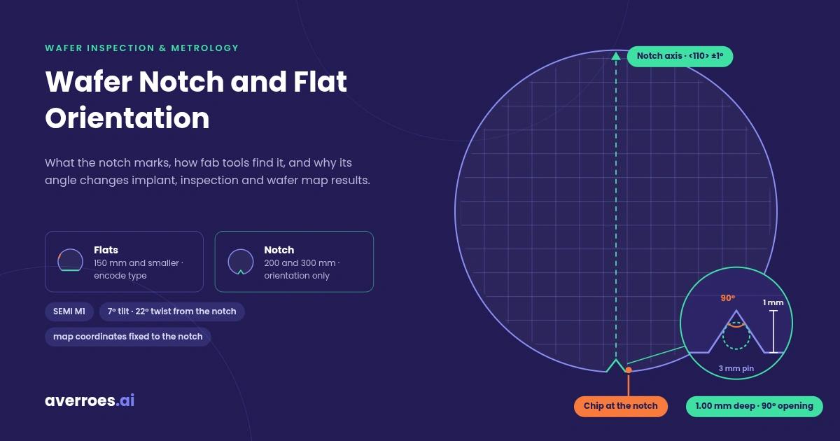
A wafer notch is a small V-shaped cut in the edge of a silicon wafer that marks its crystal orientation. On 200 mm and 300 mm wafers, SEMI M1 sets the notch at 1 mm deep with a 90° opening, centered on the <110> direction. Smaller wafers use flat edges instead. Every handling, lithography, implant and inspection tool finds the notch first, because the wafer’s crystal axes and its defect map coordinates are all referenced to it.
The notch is ground at the wafer supplier, as described in how silicon wafers are made, and read at almost every step of the semiconductor manufacturing process that follows. This guide from Averroes.ai, an AI visual inspection platform for manufacturers, covers what the notch marks, how tools find it, where its angle changes the result, and how the notch itself is inspected.
Key Notes
Flats came first: wafers up to 150 mm use primary and secondary flats, which also encode doping type. A notch encodes orientation only.
Implant angles are set from the notch: a common non-channeling setting is 7° tilt and 22° twist, with twist measured from the notch.
Inspection results depend on notch orientation: one study found pattern defect capture changed with scan orientation relative to line direction.
The notch is also an edge defect zone: its concave shape traps resist and residue, so edge tools image it separately.
What Is a Wafer Notch?
A wafer notch is a V-shaped cut ground into the edge of a semiconductor wafer to mark the direction of its crystal axes, so every tool can orient the wafer the same way. Silicon wafers look identical from every angle, but the crystal lattice inside them is not. The notch is the only physical feature that tells a robot, a stepper or an inspection stage which way the lattice runs.
Two terms need separating early. Orientation here means the wafer’s in-plane rotation, which the notch sets. It is a different property from surface orientation, the crystal plane the wafer is cut on, usually (100) for CMOS. And the wafer notch has nothing to do with “notching” in plasma etch, which is a lateral undercut at the base of an etched feature.
Wafer Flat vs Notch
An orientation flat is a straight edge ground along the length of the ingot before slicing, so every wafer cut from it carries the same flat. Wafers up to 150 mm use flats. From 200 mm onward the industry moved to the notch, because a flat removes a large segment of usable silicon and makes the wafer asymmetric in spin and thermal steps, a drawback early notch-positioning patents describe directly.
Wafer flat vs notch
Feature
Orientation Flat
Notch
Wafer sizes
Up to 150 mm
200 mm and 300 mm
Shape
Straight edge segment
Small V-shaped cut
What it marks
Crystal orientation
Crystal orientation
Encodes doping type
Yes, through the secondary flat
No
Silicon area lost
Large segment of the edge
About 1 mm at one point
How tools engage it
Flat edge against a stop
Alignment pin or edge sensing
The trade has one cost. A notch does not tell you doping type. On flatted wafers, the position of the secondary flat encoded p-type or n-type and the surface plane. On notched wafers, doping type comes from the wafer’s label, its laser mark or a measurement.
Which Direction the Wafer Notch Points
The notch axis on a standard (100) wafer is aligned to the <110> crystal direction within ±1°, as SEMI M1 specifies. That direction matters beyond alignment: (100) silicon cleaves along <110>, so a (100) wafer breaks into rectangular pieces with edges parallel and perpendicular to the notch. The lattice the notch points into is set much earlier, when the seed crystal is oriented at the start of the Czochralski process.
The comparison shows the trade in one view: the flat carries more information, but the notch costs almost no usable silicon.
Wafer Notch and Flat Specifications
SEMI M1 fixes the notch geometry for 200 mm and 300 mm wafers and the flat lengths and positions for smaller wafers, so a notch finder or flat aligner works on any compliant wafer. Diameter, thickness and resistivity sit in the same standard and are covered in silicon wafer specifications. This section covers only the orientation markers.
Wafer notch dimensions and flat lengths (SEMI M1)
Wafer Diameter
Orientation Marker
Key Dimension
Orientation
100 mm
Primary flat
32.5 ± 2.5 mm long
{110} ± 1°
125 mm
Primary flat
42.5 ± 2.5 mm long
{110} ± 1°
150 mm
Primary flat
57.5 ± 2.5 mm (47.5 ± 2.5 mm without a secondary flat)
{110} ± 1°
200 mm
Notch
1.00 mm deep, 90° opening
<110> ± 1°
300 mm
Notch
1.00 mm deep, 90° opening
<110> ± 1°
Under SEMI M1, the notch is 1.00 mm deep with a tolerance of +0.25 mm and -0.00 mm, and its opening angle is 90° with a tolerance of +5° and -1°. The notch dimensions are drawn around a 3 mm diameter alignment pin. That is why the tolerances are one-sided: a notch can be slightly deeper or wider without harm, but a shallow or narrow notch would stop the pin from seating. SEMI M1 carries two 150 mm categories: 57.5 mm for wafers with a secondary flat and 47.5 mm for wafers without one, so a 150 mm purchase spec must name its category.
Primary and Secondary Flats
A primary flat is the longer flat on a wafer of 150 mm or less, cut parallel to a {110} plane to mark crystal orientation. A secondary flat, where present, is shorter and sits at a set angle from the primary: 45°, 90° or 180° clockwise in the SEMI M1 convention. Which position appears, or whether the secondary flat is absent, encodes the doping type and surface orientation of the wafer. The full code table is in SEMI M1.
How Fab Tools Find the Wafer Notch
A wafer prealigner finds the notch by spinning the wafer and reading its edge, then computes both the notch angle and the wafer’s center offset before the wafer is placed on a process or inspection stage. Prealignment runs in front of almost every tool in a fab, often several times per process step.
Notch finding runs in 4 steps:
Center the wafer on a rotating chuck inside the prealigner or the tool’s handler.
Rotate and sample the edge with a sensor, building a profile of edge position against rotation angle.
Detect the notch as the sharp dip in that profile, and fit the circle to find the wafer center.
Correct and hand off: rotate to the target notch angle, compensate the center offset, and pass the wafer to the stage.
Three sensing methods do this work. Mechanical wafer aligners engage the notch with a pin or roller, and are common in bulk aligners that orient a full carrier of wafers at once. Optical edge sensors place a light source and a receiver across the wafer edge and read the shadow, which is the most common single-wafer method. Camera-based vision images the edge or the whole wafer and locates the notch in software.
Each method has a failure mode. Transparent substrates such as silicon carbide and some coatings weaken the contrast optical sensors rely on. A 2025 study from Hanyang University found that when an edge support partly blocks the light, brightness-based notch matching can fail outright. And a chip near the notch can be read as the notch itself, which puts the whole wafer at the wrong angle.
The takeaway: prealignment is a measurement, and like any measurement it fails on unusual substrates and damaged edges.
Why Notch Orientation Matters at Each Process Step
Notch orientation matters wherever a process interacts with the crystal lattice or with the pattern direction, because the notch is the only physical reference for both. A wafer that reaches a tool at the wrong angle may still process, but the result changes in ways the tool itself does not report.
Where notch orientation changes the result
Process Step
What the Notch Angle Sets
If the Angle Is Wrong
Lithography
Die grid against crystal axes
Grid rotated to the lattice
Ion implantation
Twist angle of the beam
Channeling, deeper dopant profile
Anisotropic etch, cleaving
Feature walls along <110>
Distorted etch profiles, bad cleaves
Defect inspection
Scan direction against lines
Changed defect capture
Wafer mapping
Map coordinate system
Rotated defect signatures
Epitaxy
Notch position on susceptor
Local thickness and backside deposits
In lithography, the notch sets coarse orientation before the stepper reads its own fine alignment marks. Notch-based pre-alignment brings the wafer close enough for those marks to be found; the layer-to-layer accuracy that follows is a separate measurement, covered in overlay metrology. The photolithography process explains where pre-alignment fits in the exposure sequence. At epitaxy, patent literature on susceptor design describes excess layer thickness and backside deposition concentrating around the notch, because process gas reaches the back surface through the cut.
Ion Implantation and Channeling
Ion implantation is the step most sensitive to notch angle. Channeling happens when ions enter along open lanes in the crystal lattice and travel deeper than intended. Implanters prevent it by setting two angles: tilt, between the beam and the wafer normal, and twist, the rotation of the wafer around its own axis, measured from the notch. A 2010 Semiconductor Digest case study reported 7° tilt with 22° twist as the typical setting. Axcelis research published in 2023 showed that near the main crystal axis, twist still changes the dopant profile through planar channeling, even at tilts of 1° or less. A wrong notch angle shifts the twist, and the implant profile shifts with it. That sensitivity is why academic work on camera-based notch-angle detection targets implanters first.
Defect Inspection Recipes
Defect inspection is the step where notch orientation is easiest to overlook. A GlobalFoundries Dresden case study presented at ISTFA 2021 traced the problem back from yield data: the link between defect density and yield on a terminal metal layer varied widely from product to product. Rotating the wafer in the defect scan tool removed the discrepancy, because extra pattern defects were captured mostly at one notch orientation relative to the layer’s dominant metal line direction. Recipe orientation is a sensitivity variable, not a handling detail. Scan setup for macro inspection and patterned inspection should record the notch orientation it was qualified at.
Wafer Maps
Every defect map, bin map and metrology map is drawn in coordinates fixed to the notch. Each fab sets its own convention for where the notch sits on the map. A wafer loaded at the wrong angle produces a rotated map, and a rotated scratch or edge signature then points to the wrong tool, chamber or handler. Wafer defect map analysis depends on that coordinate frame being right, and so do the wafer probe maps that sort dies after electrical test.
The three panels share one point: the notch angle is an input to the result, not just to the handling.
How the Wafer Notch Is Inspected
Notch inspection checks the notch for correct position and for the same defects found elsewhere on the edge, imaged as its own zone because its concave shape breaks the optics used for the rest of the bevel. It happens at two points: outgoing quality checks at the wafer supplier, and edge inspection inside the fab during the wafer inspection and metrology stage.
The first check is orientation: the notch sits where the specification and the recipe expect it. The second is condition. Onto Innovation’s 2025 note on bare wafer inspection groups the notch with the edge, inspected for orientation and for the same particle, chip and pit defects, with automatic defect classification sought to cut manual review at outgoing QA.
Inside the fab, the notch collects its own defect types. Resist pools in the cut, edge bead removal lines break around it, and chips concentrate at its corners. Edge tools image the notch with a separate optics pass. The zones of the edge, the defects each one collects and the tools that image them are covered in wafer edge and bevel inspection.
One relationship links the two jobs. A chip at the notch is both an edge defect and an alignment risk, because a notch finder can lock onto the chip instead of the notch.
Where AI Fits in Notch Detection and Inspection
AI detection models learn the notch and notch-zone defects from images the tool already captures, which keeps working where brightness thresholds fail on transparent wafers, partial occlusion or vibration. Two 2025 papers in Applied Sciences applied YOLOv8 detection models to notch-angle detection on ion implanters, including oriented bounding boxes that estimate the angle directly. Both frame the goal the same way: catch a misaligned wafer before the implant, not after.
On existing cameras, AI has two jobs around the notch:
Verify notch position against the angle the recipe expects, before processing or before a defect map is drawn. This job usually sits with the prealigner, the tool handler or a dedicated notch-detection system.
Classify notch-zone defects from edge and macro images into real defect classes and nuisance, so a residue pocket is not reviewed like a chip and a chip is not missed among residue.
Averroes.ai runs AI defect detection as an overlay on the edge, macro and automated optical inspection for wafers tools a fab or wafer supplier already owns. It trains models from 20 to 40 labeled images per defect class, with no code, and deploys on premise so wafer images stay inside the customer environment. Defect classification then sorts notch-zone detections into classes that can be trended by tool, lot and supplier.
What Is Hiding in the Notch?
Test AI defect detection on your own edge and notch images
Frequently Asked Questions
Why do silicon wafers have a notch?
Silicon wafers have a notch to mark the direction of their crystal axes, so every tool orients the wafer the same way. Lithography, implant, etch and inspection results all depend on that orientation. Wafers of 200 mm and larger use a notch instead of a flat because it removes far less usable silicon.
What is the difference between a wafer flat and a notch?
A wafer flat is a straight edge segment used on wafers up to 150 mm, and a secondary flat can encode doping type and surface orientation. A notch is a small V-shaped cut used on 200 mm and 300 mm wafers. It marks crystal orientation only and wastes far less of the wafer.
Which direction does the wafer notch point?
On a standard (100) silicon wafer, the notch axis points along the <110> crystal direction within ±1°, as SEMI M1 specifies. The same direction is the natural cleave line of (100) silicon, so a broken wafer splits into pieces with edges parallel and perpendicular to the notch.
How deep is a wafer notch?
Under SEMI M1, a notch on a 200 mm or 300 mm wafer is 1.00 mm deep, with a tolerance of +0.25 mm and -0.00 mm. Its opening angle is 90°, with a tolerance of +5° and -1°. The geometry is drawn around a 3 mm alignment pin.
Can you tell a wafer’s doping type from its notch?
No. A notch marks crystal orientation only. On wafers up to 150 mm, the position of the secondary flat encoded doping type, but notched wafers carry no such code. Doping type comes from the wafer label, its laser mark, or a measurement such as a hot-point probe test.
Do silicon carbide wafers use notches or flats?
Silicon carbide wafers use both, split by size much like silicon. Under SEMI M55-0921 and supplier specifications such as Wolfspeed’s, 150 mm SiC wafers typically carry a primary flat and 200 mm SiC wafers carry a notch. A 200 mm SiC notch is 1.0 mm deep, but its orientation tolerance is ±5°, looser than silicon’s ±1°.






A wafer notch is a small V-shaped cut in the edge of a silicon wafer that marks its crystal orientation. On 200 mm and 300 mm wafers, SEMI M1 sets the notch at 1 mm deep with a 90° opening, centered on the <110> direction. Smaller wafers use flat edges instead. Every handling, lithography, implant and inspection tool finds the notch first, because the wafer’s crystal axes and its defect map coordinates are all referenced to it.
The notch is ground at the wafer supplier, as described in how silicon wafers are made, and read at almost every step of the semiconductor manufacturing process that follows. This guide from Averroes.ai, an AI visual inspection platform for manufacturers, covers what the notch marks, how tools find it, where its angle changes the result, and how the notch itself is inspected.
Key Notes
What Is a Wafer Notch?
A wafer notch is a V-shaped cut ground into the edge of a semiconductor wafer to mark the direction of its crystal axes, so every tool can orient the wafer the same way. Silicon wafers look identical from every angle, but the crystal lattice inside them is not. The notch is the only physical feature that tells a robot, a stepper or an inspection stage which way the lattice runs.
Two terms need separating early. Orientation here means the wafer’s in-plane rotation, which the notch sets. It is a different property from surface orientation, the crystal plane the wafer is cut on, usually (100) for CMOS. And the wafer notch has nothing to do with “notching” in plasma etch, which is a lateral undercut at the base of an etched feature.
Wafer Flat vs Notch
An orientation flat is a straight edge ground along the length of the ingot before slicing, so every wafer cut from it carries the same flat. Wafers up to 150 mm use flats. From 200 mm onward the industry moved to the notch, because a flat removes a large segment of usable silicon and makes the wafer asymmetric in spin and thermal steps, a drawback early notch-positioning patents describe directly.
Wafer flat vs notch
The trade has one cost. A notch does not tell you doping type. On flatted wafers, the position of the secondary flat encoded p-type or n-type and the surface plane. On notched wafers, doping type comes from the wafer’s label, its laser mark or a measurement.
Which Direction the Wafer Notch Points
The notch axis on a standard (100) wafer is aligned to the <110> crystal direction within ±1°, as SEMI M1 specifies. That direction matters beyond alignment: (100) silicon cleaves along <110>, so a (100) wafer breaks into rectangular pieces with edges parallel and perpendicular to the notch. The lattice the notch points into is set much earlier, when the seed crystal is oriented at the start of the Czochralski process.
The comparison shows the trade in one view: the flat carries more information, but the notch costs almost no usable silicon.
Wafer Notch and Flat Specifications
SEMI M1 fixes the notch geometry for 200 mm and 300 mm wafers and the flat lengths and positions for smaller wafers, so a notch finder or flat aligner works on any compliant wafer. Diameter, thickness and resistivity sit in the same standard and are covered in silicon wafer specifications. This section covers only the orientation markers.
Wafer notch dimensions and flat lengths (SEMI M1)
Under SEMI M1, the notch is 1.00 mm deep with a tolerance of +0.25 mm and -0.00 mm, and its opening angle is 90° with a tolerance of +5° and -1°. The notch dimensions are drawn around a 3 mm diameter alignment pin. That is why the tolerances are one-sided: a notch can be slightly deeper or wider without harm, but a shallow or narrow notch would stop the pin from seating. SEMI M1 carries two 150 mm categories: 57.5 mm for wafers with a secondary flat and 47.5 mm for wafers without one, so a 150 mm purchase spec must name its category.
Primary and Secondary Flats
A primary flat is the longer flat on a wafer of 150 mm or less, cut parallel to a {110} plane to mark crystal orientation. A secondary flat, where present, is shorter and sits at a set angle from the primary: 45°, 90° or 180° clockwise in the SEMI M1 convention. Which position appears, or whether the secondary flat is absent, encodes the doping type and surface orientation of the wafer. The full code table is in SEMI M1.
How Fab Tools Find the Wafer Notch
A wafer prealigner finds the notch by spinning the wafer and reading its edge, then computes both the notch angle and the wafer’s center offset before the wafer is placed on a process or inspection stage. Prealignment runs in front of almost every tool in a fab, often several times per process step.
Notch finding runs in 4 steps:
Three sensing methods do this work. Mechanical wafer aligners engage the notch with a pin or roller, and are common in bulk aligners that orient a full carrier of wafers at once. Optical edge sensors place a light source and a receiver across the wafer edge and read the shadow, which is the most common single-wafer method. Camera-based vision images the edge or the whole wafer and locates the notch in software.
Each method has a failure mode. Transparent substrates such as silicon carbide and some coatings weaken the contrast optical sensors rely on. A 2025 study from Hanyang University found that when an edge support partly blocks the light, brightness-based notch matching can fail outright. And a chip near the notch can be read as the notch itself, which puts the whole wafer at the wrong angle.
The takeaway: prealignment is a measurement, and like any measurement it fails on unusual substrates and damaged edges.
Why Notch Orientation Matters at Each Process Step
Notch orientation matters wherever a process interacts with the crystal lattice or with the pattern direction, because the notch is the only physical reference for both. A wafer that reaches a tool at the wrong angle may still process, but the result changes in ways the tool itself does not report.
Where notch orientation changes the result
In lithography, the notch sets coarse orientation before the stepper reads its own fine alignment marks. Notch-based pre-alignment brings the wafer close enough for those marks to be found; the layer-to-layer accuracy that follows is a separate measurement, covered in overlay metrology. The photolithography process explains where pre-alignment fits in the exposure sequence. At epitaxy, patent literature on susceptor design describes excess layer thickness and backside deposition concentrating around the notch, because process gas reaches the back surface through the cut.
Ion Implantation and Channeling
Ion implantation is the step most sensitive to notch angle. Channeling happens when ions enter along open lanes in the crystal lattice and travel deeper than intended. Implanters prevent it by setting two angles: tilt, between the beam and the wafer normal, and twist, the rotation of the wafer around its own axis, measured from the notch. A 2010 Semiconductor Digest case study reported 7° tilt with 22° twist as the typical setting. Axcelis research published in 2023 showed that near the main crystal axis, twist still changes the dopant profile through planar channeling, even at tilts of 1° or less. A wrong notch angle shifts the twist, and the implant profile shifts with it. That sensitivity is why academic work on camera-based notch-angle detection targets implanters first.
Defect Inspection Recipes
Defect inspection is the step where notch orientation is easiest to overlook. A GlobalFoundries Dresden case study presented at ISTFA 2021 traced the problem back from yield data: the link between defect density and yield on a terminal metal layer varied widely from product to product. Rotating the wafer in the defect scan tool removed the discrepancy, because extra pattern defects were captured mostly at one notch orientation relative to the layer’s dominant metal line direction. Recipe orientation is a sensitivity variable, not a handling detail. Scan setup for macro inspection and patterned inspection should record the notch orientation it was qualified at.
Wafer Maps
Every defect map, bin map and metrology map is drawn in coordinates fixed to the notch. Each fab sets its own convention for where the notch sits on the map. A wafer loaded at the wrong angle produces a rotated map, and a rotated scratch or edge signature then points to the wrong tool, chamber or handler. Wafer defect map analysis depends on that coordinate frame being right, and so do the wafer probe maps that sort dies after electrical test.
The three panels share one point: the notch angle is an input to the result, not just to the handling.
How the Wafer Notch Is Inspected
Notch inspection checks the notch for correct position and for the same defects found elsewhere on the edge, imaged as its own zone because its concave shape breaks the optics used for the rest of the bevel. It happens at two points: outgoing quality checks at the wafer supplier, and edge inspection inside the fab during the wafer inspection and metrology stage.
The first check is orientation: the notch sits where the specification and the recipe expect it. The second is condition. Onto Innovation’s 2025 note on bare wafer inspection groups the notch with the edge, inspected for orientation and for the same particle, chip and pit defects, with automatic defect classification sought to cut manual review at outgoing QA.
Inside the fab, the notch collects its own defect types. Resist pools in the cut, edge bead removal lines break around it, and chips concentrate at its corners. Edge tools image the notch with a separate optics pass. The zones of the edge, the defects each one collects and the tools that image them are covered in wafer edge and bevel inspection.
One relationship links the two jobs. A chip at the notch is both an edge defect and an alignment risk, because a notch finder can lock onto the chip instead of the notch.
Where AI Fits in Notch Detection and Inspection
AI detection models learn the notch and notch-zone defects from images the tool already captures, which keeps working where brightness thresholds fail on transparent wafers, partial occlusion or vibration. Two 2025 papers in Applied Sciences applied YOLOv8 detection models to notch-angle detection on ion implanters, including oriented bounding boxes that estimate the angle directly. Both frame the goal the same way: catch a misaligned wafer before the implant, not after.
On existing cameras, AI has two jobs around the notch:
Averroes.ai runs AI defect detection as an overlay on the edge, macro and automated optical inspection for wafers tools a fab or wafer supplier already owns. It trains models from 20 to 40 labeled images per defect class, with no code, and deploys on premise so wafer images stay inside the customer environment. Defect classification then sorts notch-zone detections into classes that can be trended by tool, lot and supplier.
What Is Hiding in the Notch?
Test AI defect detection on your own edge and notch images
Frequently Asked Questions
Why do silicon wafers have a notch?
Silicon wafers have a notch to mark the direction of their crystal axes, so every tool orients the wafer the same way. Lithography, implant, etch and inspection results all depend on that orientation. Wafers of 200 mm and larger use a notch instead of a flat because it removes far less usable silicon.
What is the difference between a wafer flat and a notch?
A wafer flat is a straight edge segment used on wafers up to 150 mm, and a secondary flat can encode doping type and surface orientation. A notch is a small V-shaped cut used on 200 mm and 300 mm wafers. It marks crystal orientation only and wastes far less of the wafer.
Which direction does the wafer notch point?
On a standard (100) silicon wafer, the notch axis points along the <110> crystal direction within ±1°, as SEMI M1 specifies. The same direction is the natural cleave line of (100) silicon, so a broken wafer splits into pieces with edges parallel and perpendicular to the notch.
How deep is a wafer notch?
Under SEMI M1, a notch on a 200 mm or 300 mm wafer is 1.00 mm deep, with a tolerance of +0.25 mm and -0.00 mm. Its opening angle is 90°, with a tolerance of +5° and -1°. The geometry is drawn around a 3 mm alignment pin.
Can you tell a wafer’s doping type from its notch?
No. A notch marks crystal orientation only. On wafers up to 150 mm, the position of the secondary flat encoded doping type, but notched wafers carry no such code. Doping type comes from the wafer label, its laser mark, or a measurement such as a hot-point probe test.
Do silicon carbide wafers use notches or flats?
Silicon carbide wafers use both, split by size much like silicon. Under SEMI M55-0921 and supplier specifications such as Wolfspeed’s, 150 mm SiC wafers typically carry a primary flat and 200 mm SiC wafers carry a notch. A 200 mm SiC notch is 1.0 mm deep, but its orientation tolerance is ±5°, looser than silicon’s ±1°.