Wafer Edge and Bevel Inspection: Tools, Techniques and Yield Impact in Semiconductor Fabs
Averroes
Nov 03, 2026
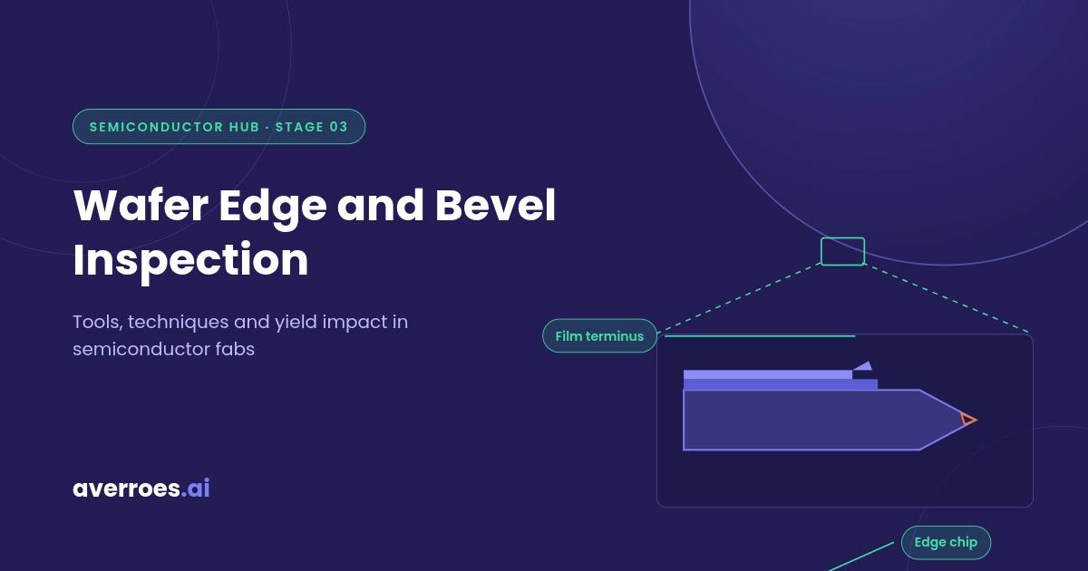
Wafer edge and bevel inspection images the outermost zones of a semiconductor wafer, the edge top area, top bevel, apex, bottom bevel and edge bottom area, for chips, cracks, film delamination and residue. In a fab it runs on dedicated 360-degree edge cameras or edge modules on macro inspection tools, because edge defects rarely stay at the edge: flakes and particles born there migrate inward to the active area and cost yield.
Edge inspection runs inside Stage 03 of the 12-stage semiconductor manufacturing process, on an edge the wafer supplier ground, polished and inspected once already. This guide from Averroes.ai, an AI visual inspection platform for manufacturers, covers the edge zones and what forms in each, where fab-side edge defects come from, edge bead removal and its verification, the edge die economics, and how the tools and the AI layer on top of them work.
Key Notes
The wafer edge divides into five named zones plus the notch, and each zone collects its own defect types from its own process steps.
Edge defects propagate inward: a flaking film at the bevel becomes front-side particles dies away from where it started.
Edge bead removal (EBR) sets the film boundary at the edge, and edge inspection is how its line, width and residue are verified.
Edge dies sit against the edge exclusion ring, so edge defect control decides whether the outermost die ring ships or scraps.
The Zones of a Wafer Edge
A wafer edge is divided into five inspection zones: the edge top area on the frontside periphery, the top bevel, the apex at the outermost point, the bottom bevel, and the edge bottom area on the backside periphery. The naming is standard across edge inspection tools, and each zone is a different surface with its own defect population.
Edge top area (ET). The outermost ring of the frontside, where the device pattern gives way to the periphery. This is where film edges terminate, where the EBR line is cut, and where resist and slurry residue settle first.
Top edge bevel (TE). The downward-sloping face between the frontside and the apex. Films wrap partway down it and end unevenly, so flaking and delamination concentrate here, and handling chips mark it.
Apex. The outermost curved tip of the wafer. It touches cassettes, grippers and containers more than any other surface, which makes it the collection point for chips, microcracks and embedded particles.
Bottom edge bevel (BE). The upward-sloping face on the underside. Backside films and residues end here, and flaking from this zone drops particles onto chucks rather than onto the wafer itself, which is how it contaminates the next wafer instead.
Edge bottom area (EB). The outermost ring of the backside, bordering the territory of backside wafer inspection; contamination that settles here tilts the wafer on vacuum chucks the same way backside particles do.
The Notch
The wafer notch is the small cutout ground into the edge during ingot shaping to mark crystal orientation, and it stays part of the edge for the wafer’s whole life. Its concave geometry makes it the hardest edge surface to coat, to strip and to image: resist pools in it, EBR lines break around it, and chips concentrate at its corners. Edge tools image the notch as its own zone with its own optics pass.
Wafer edge zones and what forms in each
Zone
Where It Is
Typical Defects
Main Source
Edge top area
Frontside periphery
Residue, EBR defects, film edges
Coating, EBR, polish
Top edge bevel
Upper sloped face
Delamination, flaking, chips
Film terminus, handling
Apex
Outermost tip
Chips, microcracks, particles
Grippers, cassettes
Bottom edge bevel
Lower sloped face
Flaking, residue
Backside films, chemistry
Edge bottom area
Backside periphery
Contamination, particles
Chucks, handling
Notch
Orientation cutout
Residue, broken EBR line, chips
Coating, EBR, contact
The map’s takeaway in one line: the edge is not one surface but six, and every one of them collects defects from a different direction.
Where Edge Defects Come From in the Fab
Fab-side edge defects are created by the films, chemistries and handling the wafer accumulates after it arrives, on an edge the supplier already ground and inspected. The supplier’s edge gate, described in how silicon wafers are made, caught the grinding-era chips and cracks before shipping. Everything that appears afterward is the fab’s own doing, and it comes from three directions.
The film terminus. Every film deposited on the wafer ends somewhere, and it ends at the edge. The termination is where film stress concentrates, where adhesion is weakest and where coverage is least controlled, so delamination starts at the edge before the face of the film shows anything. The same stress that thin film inspection tracks as blistering on the face arrives at the bevel first, with less margin: a lifted film edge flakes with the next thermal step or the next contact.
Edge chemistry. The edge is where coating meets stripping. EBR solvent cuts its line through the resist rim, etch chemistries attack exposed film edges that the pattern protects everywhere else, and slurry from planarization wraps the bevel and dries where rinsing is least effective. Residue that survives here sheds for weeks.
Mechanical contact. Grippers, chucks, cassettes and transport systems touch the wafer only at its edge, by design, which means every handoff in a thousand-step flow is an edge contact. Chips and microcracks accumulate with the handling count, and a bevel microcrack that stays dormant at room temperature can propagate under the next furnace ramp.
The reason all of this earns its own inspection is the migration path. A flake released at the bevel does not stay at the bevel: it lands on a chuck, rides a transfer arm, or falls onto the active area dies away from where it started. By the time it is found by frontside inspection, it looks like a particle excursion from nowhere. Edge defects are upstream causes wearing a downstream disguise, and inspecting the edge is how the disguise comes off.
The panel’s takeaway in one line: three different process families create edge defects, and all three send their debris inward.
Edge Bead Removal, and How Inspection Verifies It
Edge bead removal (EBR) strips the bead of resist or film that accumulates at the wafer’s rim during coating, cutting a clean boundary a few millimeters from the edge. Spin coating piles material at the rim as it spreads, and a bead left in place dries thick, cracks, and flakes inside the track and every tool after it. EBR removes it with a solvent stream dispensed at the rotating rim, or with an exposure pass that clears the rim at develop.
EBR is a process step, not an inspection. Edge inspection is how its result is verified, and the checklist is specific:
Line placement and width. The EBR line position sets how much edge the film gives up. A line drifting outward leaves bead; a line drifting inward consumes active area.
Line quality. A rough or scalloped EBR line sheds at its own ragged boundary and complicates every film that terminates near it.
Residual bead. Incomplete removal leaves arcs of thick material that flake under thermal stress, the exact failure EBR exists to prevent.
Overspray and splashback. Solvent reaching the active area thins resist where dies live.
The notch. The line geometry breaks around the notch cutout, so residue and incomplete removal concentrate there.
EBR drift is also the canonical edge monitoring case. The line creeping outward or roughening over a week is a slow excursion that no single-wafer inspection flags as a failure, and that zone-level trending catches before the flaking starts. That distinction, defect found versus drift trended, is where this page’s final section picks up.
Edge Exclusion and Edge Die Yield
Edge exclusion is the ring at the wafer’s rim where no product dies are placed, because film uniformity, overlay and defectivity all degrade toward the edge. Every process in the fab is least controlled at the rim: films thin or thicken, planarization rolls off, exposure fields fall partly off the wafer, and the defect sources above all live there. The exclusion ring concedes that territory.
The concession is expensive. The excluded ring multiplied around the wafer’s circumference is purchased silicon that ships nothing, and because area scales with radius, millimeters at the rim carry a disproportionate share of the wafer. Tightening edge exclusion adds a full ring of candidate dies, which is why fabs keep testing whether the edge can hold more product.
Whether it can is an edge defectivity question. Edge dies yield worse than center dies for reasons this page has already toured: partial exposure fields, film and polish non-uniformity at the rim, and proximity to every edge defect source. Edge inspection data is the evidence base for the decision: zone-level defect rates, EBR line stability and bevel condition are what say whether the exclusion line can move outward, or must move in.
The map’s takeaway in one line: the exclusion line is an economic decision, and edge inspection data is what the decision runs on.
How Edge Inspection Tools Work
Edge inspection tools rotate the wafer past a set of cameras angled at the top bevel, apex and bottom bevel, building a 360-degree composite image of every zone. The geometry is the whole problem: the edge is curved, specular and multi-surfaced, so frontside inspection optics looking straight down see almost none of it. Dedicated edge modules and the edge stations on macro inspection tools solve it with multiple viewing angles captured per revolution, an approach demonstrated for automated 300 mm edge and bevel inspection as early as Morillo’s 2005 IEEE work and still the architecture Semiconductor Engineering describes on current platforms.
Two tool families divide the edge, and the split answers a common equipment question:
Optical edge inspection finds and classifies defects: chips, flakes, delamination, residue, EBR faults, across the zones and the notch. Brightfield and darkfield channels on the same rotation catch topographic and scattering defects respectively.
AFM and areal profilometry measure the bevel itself: shape, angle and roughness, as in the areal-imaging method published via ASME in 2024. This is edge metrology rather than inspection, and it is what qualifies bevel geometry where it has become a bonding parameter in advanced packaging.
One boundary completes the toolscape: bevel etch and edge cleaning systems remove films and contamination from the edge, and they rank on edge inspection queries, but they are remediation, not inspection. Inspection is what decides whether, where and how often they are needed.
Where AI Fits in Edge and Bevel Inspection
AI defect detection finds and classifies edge defects on the 360-degree composite images edge tools already produce, across curved surfaces and film-terminus backgrounds that defeat fixed rules. The edge is the hardest background in the fab: every zone presents a different surface, every layer changes what the edge looks like, and the film terminus puts legitimate film boundaries exactly where defects hide. A fixed threshold either flags every film edge on the wafer or misses the flake sitting beside one.
Learned detection changes the terms. A model trained on the fab’s own edge imagery learns what each zone looks like per layer, which lets it hold sensitivity at the terminus instead of trading it away, and classify what it finds into the classes that drive action: delamination, chip, residue, EBR fault, nuisance.
Classification is also what makes the monitoring loop work. Trending classified edge defects by zone, layer and lot turns the slow failures this page has collected, EBR drift, gripper wear, a film that has started releasing at its terminus, into named excursions with a location and a trend line, before their debris reaches the active area. That is the propagate-inward problem answered at its source.
Averroes.ai runs AI defect detection on the edge and bevel imagery from the tools a fab already owns, trained from 20 to 40 labeled images per defect class, with no code, deployed on premise so wafer imagery stays inside the fab. Defect monitoring trends the classified output by zone, layer and lot. Both run as an overlay on the installed edge tools, never a replacement for them.
The frame’s takeaway in one line: the cameras solve the geometry, and the model solves the background.
Is the Edge Costing You the Outer Die Ring?
See AI defect detection on your own wafer edge and bevel images
Frequently Asked Questions
What is wafer edge and bevel inspection?
Wafer edge and bevel inspection images the outermost zones of a semiconductor wafer, the edge top area, both bevels, the apex and the edge bottom area, for chips, cracks, delamination and residue. It runs on 360-degree edge cameras or macro tool edge modules, because defects born at the edge migrate inward and cost yield.
What are the zones of a wafer edge?
The wafer edge divides into five zones: the edge top area on the frontside periphery, the top edge bevel, the apex at the outermost tip, the bottom edge bevel, and the edge bottom area on the backside periphery. The notch is imaged as a sixth zone of its own, and each zone carries its own defect types.
What is edge bead removal?
Edge bead removal (EBR) strips the thick bead of resist or film that spin coating piles up at the wafer’s rim, cutting a clean boundary a few millimeters from the edge. Left in place, the bead cracks and flakes inside process tools. Edge inspection verifies the EBR result: line placement, width, roughness, residual bead and overspray.
What is edge exclusion on a wafer?
Edge exclusion is the ring at the wafer’s rim where no product dies are placed, because films, overlay and defectivity all degrade toward the edge. The ring is purchased silicon that ships nothing, so fabs tighten it when edge inspection data shows the defectivity and uniformity at the rim can support another ring of dies.
Why do edge dies yield worse than center dies?
Edge dies sit where every process is least controlled: exposure fields fall partly off the wafer, films and planarization roll off toward the rim, and the edge’s own defect sources, flaking film termini, EBR faults and handling chips, are closest. Edge inspection and zone trending are how fabs decide whether the outermost ring can ship.
What is the wafer notch for?
The notch is the small cutout ground into the wafer’s edge during ingot shaping to mark crystal orientation, so every tool afterward can rotate the wafer to a known angle. It is also the hardest edge geometry to inspect: coating pools in it, EBR lines break around it, and chips concentrate at its corners.








Wafer edge and bevel inspection images the outermost zones of a semiconductor wafer, the edge top area, top bevel, apex, bottom bevel and edge bottom area, for chips, cracks, film delamination and residue. In a fab it runs on dedicated 360-degree edge cameras or edge modules on macro inspection tools, because edge defects rarely stay at the edge: flakes and particles born there migrate inward to the active area and cost yield.
Edge inspection runs inside Stage 03 of the 12-stage semiconductor manufacturing process, on an edge the wafer supplier ground, polished and inspected once already. This guide from Averroes.ai, an AI visual inspection platform for manufacturers, covers the edge zones and what forms in each, where fab-side edge defects come from, edge bead removal and its verification, the edge die economics, and how the tools and the AI layer on top of them work.
Key Notes
The Zones of a Wafer Edge
A wafer edge is divided into five inspection zones: the edge top area on the frontside periphery, the top bevel, the apex at the outermost point, the bottom bevel, and the edge bottom area on the backside periphery. The naming is standard across edge inspection tools, and each zone is a different surface with its own defect population.
Edge top area (ET). The outermost ring of the frontside, where the device pattern gives way to the periphery. This is where film edges terminate, where the EBR line is cut, and where resist and slurry residue settle first.
Top edge bevel (TE). The downward-sloping face between the frontside and the apex. Films wrap partway down it and end unevenly, so flaking and delamination concentrate here, and handling chips mark it.
Apex. The outermost curved tip of the wafer. It touches cassettes, grippers and containers more than any other surface, which makes it the collection point for chips, microcracks and embedded particles.
Bottom edge bevel (BE). The upward-sloping face on the underside. Backside films and residues end here, and flaking from this zone drops particles onto chucks rather than onto the wafer itself, which is how it contaminates the next wafer instead.
Edge bottom area (EB). The outermost ring of the backside, bordering the territory of backside wafer inspection; contamination that settles here tilts the wafer on vacuum chucks the same way backside particles do.
The Notch
The wafer notch is the small cutout ground into the edge during ingot shaping to mark crystal orientation, and it stays part of the edge for the wafer’s whole life. Its concave geometry makes it the hardest edge surface to coat, to strip and to image: resist pools in it, EBR lines break around it, and chips concentrate at its corners. Edge tools image the notch as its own zone with its own optics pass.
Wafer edge zones and what forms in each
The map’s takeaway in one line: the edge is not one surface but six, and every one of them collects defects from a different direction.
Where Edge Defects Come From in the Fab
Fab-side edge defects are created by the films, chemistries and handling the wafer accumulates after it arrives, on an edge the supplier already ground and inspected. The supplier’s edge gate, described in how silicon wafers are made, caught the grinding-era chips and cracks before shipping. Everything that appears afterward is the fab’s own doing, and it comes from three directions.
The film terminus. Every film deposited on the wafer ends somewhere, and it ends at the edge. The termination is where film stress concentrates, where adhesion is weakest and where coverage is least controlled, so delamination starts at the edge before the face of the film shows anything. The same stress that thin film inspection tracks as blistering on the face arrives at the bevel first, with less margin: a lifted film edge flakes with the next thermal step or the next contact.
Edge chemistry. The edge is where coating meets stripping. EBR solvent cuts its line through the resist rim, etch chemistries attack exposed film edges that the pattern protects everywhere else, and slurry from planarization wraps the bevel and dries where rinsing is least effective. Residue that survives here sheds for weeks.
Mechanical contact. Grippers, chucks, cassettes and transport systems touch the wafer only at its edge, by design, which means every handoff in a thousand-step flow is an edge contact. Chips and microcracks accumulate with the handling count, and a bevel microcrack that stays dormant at room temperature can propagate under the next furnace ramp.
The reason all of this earns its own inspection is the migration path. A flake released at the bevel does not stay at the bevel: it lands on a chuck, rides a transfer arm, or falls onto the active area dies away from where it started. By the time it is found by frontside inspection, it looks like a particle excursion from nowhere. Edge defects are upstream causes wearing a downstream disguise, and inspecting the edge is how the disguise comes off.
The panel’s takeaway in one line: three different process families create edge defects, and all three send their debris inward.
Edge Bead Removal, and How Inspection Verifies It
Edge bead removal (EBR) strips the bead of resist or film that accumulates at the wafer’s rim during coating, cutting a clean boundary a few millimeters from the edge. Spin coating piles material at the rim as it spreads, and a bead left in place dries thick, cracks, and flakes inside the track and every tool after it. EBR removes it with a solvent stream dispensed at the rotating rim, or with an exposure pass that clears the rim at develop.
EBR is a process step, not an inspection. Edge inspection is how its result is verified, and the checklist is specific:
EBR drift is also the canonical edge monitoring case. The line creeping outward or roughening over a week is a slow excursion that no single-wafer inspection flags as a failure, and that zone-level trending catches before the flaking starts. That distinction, defect found versus drift trended, is where this page’s final section picks up.
Edge Exclusion and Edge Die Yield
Edge exclusion is the ring at the wafer’s rim where no product dies are placed, because film uniformity, overlay and defectivity all degrade toward the edge. Every process in the fab is least controlled at the rim: films thin or thicken, planarization rolls off, exposure fields fall partly off the wafer, and the defect sources above all live there. The exclusion ring concedes that territory.
The concession is expensive. The excluded ring multiplied around the wafer’s circumference is purchased silicon that ships nothing, and because area scales with radius, millimeters at the rim carry a disproportionate share of the wafer. Tightening edge exclusion adds a full ring of candidate dies, which is why fabs keep testing whether the edge can hold more product.
Whether it can is an edge defectivity question. Edge dies yield worse than center dies for reasons this page has already toured: partial exposure fields, film and polish non-uniformity at the rim, and proximity to every edge defect source. Edge inspection data is the evidence base for the decision: zone-level defect rates, EBR line stability and bevel condition are what say whether the exclusion line can move outward, or must move in.
The map’s takeaway in one line: the exclusion line is an economic decision, and edge inspection data is what the decision runs on.
How Edge Inspection Tools Work
Edge inspection tools rotate the wafer past a set of cameras angled at the top bevel, apex and bottom bevel, building a 360-degree composite image of every zone. The geometry is the whole problem: the edge is curved, specular and multi-surfaced, so frontside inspection optics looking straight down see almost none of it. Dedicated edge modules and the edge stations on macro inspection tools solve it with multiple viewing angles captured per revolution, an approach demonstrated for automated 300 mm edge and bevel inspection as early as Morillo’s 2005 IEEE work and still the architecture Semiconductor Engineering describes on current platforms.
Two tool families divide the edge, and the split answers a common equipment question:
One boundary completes the toolscape: bevel etch and edge cleaning systems remove films and contamination from the edge, and they rank on edge inspection queries, but they are remediation, not inspection. Inspection is what decides whether, where and how often they are needed.
Where AI Fits in Edge and Bevel Inspection
AI defect detection finds and classifies edge defects on the 360-degree composite images edge tools already produce, across curved surfaces and film-terminus backgrounds that defeat fixed rules. The edge is the hardest background in the fab: every zone presents a different surface, every layer changes what the edge looks like, and the film terminus puts legitimate film boundaries exactly where defects hide. A fixed threshold either flags every film edge on the wafer or misses the flake sitting beside one.
Learned detection changes the terms. A model trained on the fab’s own edge imagery learns what each zone looks like per layer, which lets it hold sensitivity at the terminus instead of trading it away, and classify what it finds into the classes that drive action: delamination, chip, residue, EBR fault, nuisance.
Classification is also what makes the monitoring loop work. Trending classified edge defects by zone, layer and lot turns the slow failures this page has collected, EBR drift, gripper wear, a film that has started releasing at its terminus, into named excursions with a location and a trend line, before their debris reaches the active area. That is the propagate-inward problem answered at its source.
Averroes.ai runs AI defect detection on the edge and bevel imagery from the tools a fab already owns, trained from 20 to 40 labeled images per defect class, with no code, deployed on premise so wafer imagery stays inside the fab. Defect monitoring trends the classified output by zone, layer and lot. Both run as an overlay on the installed edge tools, never a replacement for them.
The frame’s takeaway in one line: the cameras solve the geometry, and the model solves the background.
Is the Edge Costing You the Outer Die Ring?
See AI defect detection on your own wafer edge and bevel images
Frequently Asked Questions
What is wafer edge and bevel inspection?
Wafer edge and bevel inspection images the outermost zones of a semiconductor wafer, the edge top area, both bevels, the apex and the edge bottom area, for chips, cracks, delamination and residue. It runs on 360-degree edge cameras or macro tool edge modules, because defects born at the edge migrate inward and cost yield.
What are the zones of a wafer edge?
The wafer edge divides into five zones: the edge top area on the frontside periphery, the top edge bevel, the apex at the outermost tip, the bottom edge bevel, and the edge bottom area on the backside periphery. The notch is imaged as a sixth zone of its own, and each zone carries its own defect types.
What is edge bead removal?
Edge bead removal (EBR) strips the thick bead of resist or film that spin coating piles up at the wafer’s rim, cutting a clean boundary a few millimeters from the edge. Left in place, the bead cracks and flakes inside process tools. Edge inspection verifies the EBR result: line placement, width, roughness, residual bead and overspray.
What is edge exclusion on a wafer?
Edge exclusion is the ring at the wafer’s rim where no product dies are placed, because films, overlay and defectivity all degrade toward the edge. The ring is purchased silicon that ships nothing, so fabs tighten it when edge inspection data shows the defectivity and uniformity at the rim can support another ring of dies.
Why do edge dies yield worse than center dies?
Edge dies sit where every process is least controlled: exposure fields fall partly off the wafer, films and planarization roll off toward the rim, and the edge’s own defect sources, flaking film termini, EBR faults and handling chips, are closest. Edge inspection and zone trending are how fabs decide whether the outermost ring can ship.
What is the wafer notch for?
The notch is the small cutout ground into the wafer’s edge during ingot shaping to mark crystal orientation, so every tool afterward can rotate the wafer to a known angle. It is also the hardest edge geometry to inspect: coating pools in it, EBR lines break around it, and chips concentrate at its corners.