Semiconductor Defect Annotation: How Fab Teams Label Defect Data Consistently
Averroes
Updated11 min read
Table of contents7 sections
Semiconductor defect annotation is the assignment of defect classes to inspection images, review images and wafer maps so a classification model can learn them. Its quality depends on agreement as much as volume: a written defect taxonomy, class definitions with look-alike rules, an explicit nuisance class, and a regular check that two engineers label the same image the same way. Published wafer map studies link weaker classifiers to inconsistent expert labels.
Defect annotation feeds every inspection gate in the semiconductor manufacturing process. This guide from Averroes.ai, an AI visual inspection platform for manufacturers, sets out a defect taxonomy, an annotation guideline and a consistency loop that fab teams can run on their own data.
Key Notes
Manual labeling by engineers creates label uncertainty that published wafer bin map studies link to weaker classifiers.
WM-811K labels 172,950 of its 811,457 wafer maps, and most of the dataset is unlabeled and heavily imbalanced.
Nuisance detections need their own class: in sensitive inspections they can exceed 99% of all detected events.
A five-step consistency loop of golden set, double labeling, agreement check, adjudication and guideline update keeps a taxonomy stable.
What Is Semiconductor Defect Annotation?
Semiconductor defect annotation is a data preparation step that assigns defect classes, and where needed locations or outlines, to semiconductor inspection data, used to train and validate defect classification and detection models. In this guide “annotation” and “labeling” mean the same thing: assigning a class. Boxes and masks are named when they are meant.
Fab teams annotate three kinds of data:
Inspection and macro images. Optical images captured where an inspection tool flags a detection.
Review images. Higher-resolution SEM or optical images of a detection, taken during defect review. SEM review is covered in e-beam inspection.
The hard part is not drawing labels. It is getting engineers to agree on them. The authors of a December 2025 arXiv study on lithography defect datasets, built from 3,530 optical microscope images with 13,365 annotated defects across four classes, note that consistent real annotation depends on expert judgment and is difficult to standardize across annotators.
How Do You Build a Defect Taxonomy for Annotation?
A defect taxonomy is the controlled list of defect classes a fab labels and classifies, used to make every engineer and every model sort the same detection into the same class. The taxonomy comes before the first label, because every later disagreement traces back to how the classes were drawn. Defining what counts as a defect before training is also the first step in automatic defect recognition.
Defect taxonomy design rules
Rule
Why It Matters
Example
Split a class only when the response differs
Classes nobody acts on differently add disagreement, not value
One “particle” class unless size changes the disposition
Name by physical cause where known
Cause-based names point to a process owner
“CMP scratch” rather than “line defect”
Name by appearance where the cause is unknown
Guessing a cause bakes errors into labels
“Residue, unknown source”
Decide per image modality
Optical images cannot resolve what SEM can
Merge two SEM classes on optical data
Keep an explicit nuisance class
Gives the model a place for detections to ignore
Grain, color variation, film texture
Keep an explicit unknown class
Stops engineers forcing new defects into old classes
New pattern after a process change
Merge look-alikes the data cannot separate
Two classes that engineers split by guesswork become noise
Two pit types indistinguishable at review resolution
The tree makes one point: a usable taxonomy has two classes besides the defects themselves, one for what to ignore and one for what nobody has named yet.
Should Nuisance Detections Be a Labeled Class?
A nuisance defect is a detected event that is not relevant to yield, caused by wafer noise, system noise or harmless physical features, used as the name for everything an inspection flags that engineers do not act on. A KLA-Tencor patent on wafer defect detection (US 9,721,337, granted 2017) states that in a sensitive inspection, nuisance events can exceed 99% of detected events. A later KLA patent on multimode defect classification (US 11,668,655, granted 2023) describes nuisance outnumbering defects of interest by a factor of 1,000 or more.
Labeling nuisance as its own class teaches a model what to ignore. Without it, a classifier has to force every nuisance detection into a real defect class, and those detections become false positives. The same logic applies at the package level, where mold texture and marking variation are the nuisance class in IC package inspection.
How Do You Handle Unknown and Rare Defect Classes?
An unknown class is a holding class for detections that match no defined defect, used to collect new defect types for engineering review instead of mislabeling them. Images in the unknown class go to a review queue. Once a new type is understood, it becomes a named class with its own definition card.
Rare classes sit on a watch list until they reach a working number of examples. Data augmentation and synthetic image data generation can help fill them, but only after the class definition is settled.
What Should Semiconductor Defect Annotation Guidelines Include?
Defect annotation guidelines are the written rules that define each defect class, its look-alikes and its edge cases, used to make labels repeatable across engineers, shifts and sites. The core unit is a class definition card: one page per class that any engineer can apply without asking the person who wrote it.
Defect annotation guidelines: the class definition card
Field
What It Holds
Example: Particle on an SEM Review Image
Class name and code
One name, one code, used everywhere
Particle, code 01
Physical cause and process step
Where the defect comes from
Foreign material landing after clean or deposition
Image modality and scale
The image type the rules apply to
SEM review image at standard review field of view
Visual criteria
What must be visible to assign the class
Discrete bright body sitting on the surface, casting contrast
Size or contrast threshold
The line between this class and nuisance
Below the agreed size limit: nuisance
Look-alike classes and the deciding feature
The class it is most often confused with
Pit: dark, recessed, no body above the surface
Nuisance rule
What looks similar but is ignored
Surface grain with no distinct body
Reference image IDs
Golden set examples, including hard cases
Five clear examples, three borderline
Owner and revision date
Who decides disputes, and when rules last changed
Defect engineer, revision date
The card turns a class from an engineer’s private judgment into a rule anyone can check.
Guidelines also need an edge-case log. Every disputed image goes into it with the decision and the reason, and the decision feeds back into the card. A guideline that never changes after the first week is usually one nobody is checking against.
Why Do Engineers Label the Same Defect Differently?
Label noise is the share of training or test labels that are wrong or inconsistent, used as a measure of how far a dataset’s labels drift from the defect each sample actually shows. Even carefully curated data carries it. Northcutt, Athalye and Mueller (NeurIPS 2021) estimated at least 3.3% label errors on average across 10 widely used machine learning benchmark test sets, and at least 6% in the ImageNet validation set.
Semiconductor data adds its own causes. Park, Jang and Kim (Journal of Intelligent Manufacturing, 2021) report that manual labeling of wafer bin maps by engineers produces a high level of label uncertainty, and that label uncertainty is a major cause of lower classification performance. They trace it to labeling that is too coarse and to similar patterns split into too many classes. Noisy labels limit any classifier trained on them, which is why separating real defects reliably with AI defect classification starts with clean classes.
Causes of semiconductor defect label noise
Cause
What It Looks Like
Fix
Classes too coarse
Different defects share one label
Split where the response differs
Look-alikes over-split
Engineers guess between near-identical classes
Merge, or add a deciding feature to the card
Modality limits
Optical labels claim detail only SEM shows
Write rules per modality
Definitions drift after a process change
Old and new images labeled by different rules
Revise the card, relabel affected images
Shift and site habits
Each team applies its own threshold
Shared golden set, scheduled agreement checks
Mixed patterns on one wafer map
One map forced into one class
Allow multiple labels per map
How Noisy Are WM-811K Labels?
WM-811K is a public wafer map dataset of real production data, used as the standard benchmark for wafer map pattern classification. Wu, Jang and Chen built it from 811,457 real-world wafer maps (IEEE Transactions on Semiconductor Manufacturing, February 2015), and 172,950 of those maps carry a label across nine classes. A 2023 arXiv study notes three problems typical of manufacturing data in it: only about 20% of the maps are labeled, the labeled maps come in different sizes, and the classes are highly imbalanced.
Mixed patterns make single-class labels harder still. The MixedWM38 dataset was built with 29 mixed-pattern categories alongside 8 single patterns and a normal class. Public datasets are useful for benchmarking and pretraining, but they do not carry a fab’s own taxonomy. The nine-class taxonomy itself is explained in wafer defect map analysis.
How Do You Measure and Maintain Labeling Consistency?
Labeling consistency is the degree to which different annotators, or the same annotator over time, assign the same defect class to the same image, used to decide whether a labeled dataset is ready to train on. It is measured per class, because a dataset can agree well on particles and poorly on residues.
The defect labeling consistency loop runs in five steps:
Build a golden set. Collect reference images per class, including borderline cases, and agree their labels with the class owner.
Double-label a sample. Have two engineers label the same sample of new images independently.
Measure agreement per class. Use percent agreement, or Cohen’s kappa, which corrects agreement for what two annotators would match by chance.
Adjudicate disagreements. The class owner decides each disputed image and records the reason in the edge-case log.
Update the guideline and relabel. Revise the class definition card and relabel every image the change affects.
The loop shows that consistency is a routine, not a one-time cleanup: every guideline change sends affected labels back through it.
Ownership matters as much as the loop. Process and defect engineers own the class definitions and the golden set. Trained labelers can scale volume, as long as they are checked against the golden set. Human-in-the-loop review for general manufacturing defects is covered in defect detection using machine learning, and versioning labeled data across relabeling rounds in defect data management.
How Does AI Help Keep Defect Labels Consistent?
AI-assisted defect labeling is a workflow in which a model proposes labels for engineers to confirm, used to scale annotation while engineers keep control of the taxonomy. It helps consistency in three ways:
One rule, every shift. A trained classifier applies the agreed taxonomy the same way on every image, so shift and site habits stop leaking into new labels.
Disagreement as a signal. Where the model’s prediction conflicts with an existing label, the image is worth a second look by the class owner.
Active learning. The model sends the images it is least certain about to engineers first, so review time goes where labels are most likely to be wrong.
Averroes.ai is an AI visual inspection platform that runs as an overlay on the inspection and review tools a fab already owns, including KLA, AOI and Onto systems. Its AI labeling for manufacturing automates labeling, segmentation and training, and active learning routes the images that matter most to engineers. It trains defect classification models from 20 to 40 labeled images per defect class, with no code, and deploys on premise so defect images stay inside the fab.
Do Your Engineers Label the Same Defect the Same Way?
Test AI-assisted labeling on your own defect images
Frequently Asked Questions
What is a nuisance defect?
A nuisance defect is a detected event that is not relevant to yield, such as wafer noise, system noise or a harmless surface feature. In sensitive wafer inspections, nuisance events can exceed 99% of detections. Labeling nuisance as its own class teaches a classification model what to ignore instead of turning it into false positives.
Can WM-811K train a fab’s defect classification model?
WM-811K is useful for benchmarking and pretraining wafer map classifiers, but it rarely trains a production model on its own. Only about 20% of its 811,457 maps are labeled, its classes are imbalanced, and its nine-class taxonomy is generic. A fab still needs labeled data built on its own taxonomy.
How many images per defect class are needed?
Averroes.ai trains defect classification models from 20 to 40 labeled images per defect class. Other approaches quote hundreds or thousands. The full answer, including what pushes the number up or down, is in the guide to training data for AI defect detection.
Who should annotate semiconductor defect images?
Process and defect engineers should own the class definitions, the golden set and every disputed decision, because they know which defects need different responses. Trained labelers can then scale the volume, provided their labels are checked against the golden set and measured for agreement per class.
What is inter-annotator agreement?
Inter-annotator agreement measures how often two annotators assign the same label to the same image. Percent agreement is the simple share of matches. Cohen’s kappa corrects that share for agreement expected by chance. For defect data it should be measured per class, since agreement often differs sharply between classes.
What annotation type do SEM review images need?
SEM review images used for defect classification need a class label per image. Boxes or masks are needed only when a defect’s location, size or shape drives a decision, such as severity grading. Choosing between them is covered in the guide comparing defect classification, anomaly detection and segmentation.





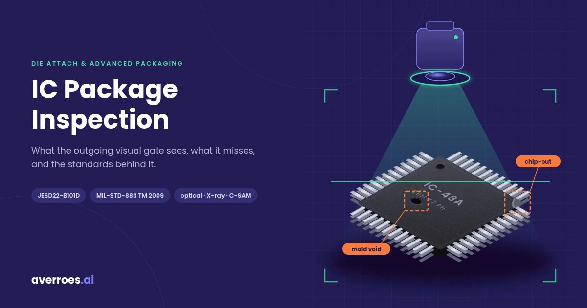


Table of contents7 sections
Semiconductor defect annotation is the assignment of defect classes to inspection images, review images and wafer maps so a classification model can learn them. Its quality depends on agreement as much as volume: a written defect taxonomy, class definitions with look-alike rules, an explicit nuisance class, and a regular check that two engineers label the same image the same way. Published wafer map studies link weaker classifiers to inconsistent expert labels.
Defect annotation feeds every inspection gate in the semiconductor manufacturing process. This guide from Averroes.ai, an AI visual inspection platform for manufacturers, sets out a defect taxonomy, an annotation guideline and a consistency loop that fab teams can run on their own data.
Key Notes
What Is Semiconductor Defect Annotation?
Semiconductor defect annotation is a data preparation step that assigns defect classes, and where needed locations or outlines, to semiconductor inspection data, used to train and validate defect classification and detection models. In this guide “annotation” and “labeling” mean the same thing: assigning a class. Boxes and masks are named when they are meant.
Fab teams annotate three kinds of data:
Annotated review images train the classifier that automatic defect classification runs on every new detection. Two related questions have their own guides. Which annotation type a method needs (class label, box or mask) is covered in defect classification vs anomaly detection vs segmentation. How many images a class needs is covered in training data for AI defect detection.
The hard part is not drawing labels. It is getting engineers to agree on them. The authors of a December 2025 arXiv study on lithography defect datasets, built from 3,530 optical microscope images with 13,365 annotated defects across four classes, note that consistent real annotation depends on expert judgment and is difficult to standardize across annotators.
How Do You Build a Defect Taxonomy for Annotation?
A defect taxonomy is the controlled list of defect classes a fab labels and classifies, used to make every engineer and every model sort the same detection into the same class. The taxonomy comes before the first label, because every later disagreement traces back to how the classes were drawn. Defining what counts as a defect before training is also the first step in automatic defect recognition.
Defect taxonomy design rules
The tree makes one point: a usable taxonomy has two classes besides the defects themselves, one for what to ignore and one for what nobody has named yet.
Should Nuisance Detections Be a Labeled Class?
A nuisance defect is a detected event that is not relevant to yield, caused by wafer noise, system noise or harmless physical features, used as the name for everything an inspection flags that engineers do not act on. A KLA-Tencor patent on wafer defect detection (US 9,721,337, granted 2017) states that in a sensitive inspection, nuisance events can exceed 99% of detected events. A later KLA patent on multimode defect classification (US 11,668,655, granted 2023) describes nuisance outnumbering defects of interest by a factor of 1,000 or more.
Labeling nuisance as its own class teaches a model what to ignore. Without it, a classifier has to force every nuisance detection into a real defect class, and those detections become false positives. The same logic applies at the package level, where mold texture and marking variation are the nuisance class in IC package inspection.
How Do You Handle Unknown and Rare Defect Classes?
An unknown class is a holding class for detections that match no defined defect, used to collect new defect types for engineering review instead of mislabeling them. Images in the unknown class go to a review queue. Once a new type is understood, it becomes a named class with its own definition card.
Rare classes sit on a watch list until they reach a working number of examples. Data augmentation and synthetic image data generation can help fill them, but only after the class definition is settled.
What Should Semiconductor Defect Annotation Guidelines Include?
Defect annotation guidelines are the written rules that define each defect class, its look-alikes and its edge cases, used to make labels repeatable across engineers, shifts and sites. The core unit is a class definition card: one page per class that any engineer can apply without asking the person who wrote it.
Defect annotation guidelines: the class definition card
The card turns a class from an engineer’s private judgment into a rule anyone can check.
Guidelines also need an edge-case log. Every disputed image goes into it with the decision and the reason, and the decision feeds back into the card. A guideline that never changes after the first week is usually one nobody is checking against.
Why Do Engineers Label the Same Defect Differently?
Label noise is the share of training or test labels that are wrong or inconsistent, used as a measure of how far a dataset’s labels drift from the defect each sample actually shows. Even carefully curated data carries it. Northcutt, Athalye and Mueller (NeurIPS 2021) estimated at least 3.3% label errors on average across 10 widely used machine learning benchmark test sets, and at least 6% in the ImageNet validation set.
Semiconductor data adds its own causes. Park, Jang and Kim (Journal of Intelligent Manufacturing, 2021) report that manual labeling of wafer bin maps by engineers produces a high level of label uncertainty, and that label uncertainty is a major cause of lower classification performance. They trace it to labeling that is too coarse and to similar patterns split into too many classes. Noisy labels limit any classifier trained on them, which is why separating real defects reliably with AI defect classification starts with clean classes.
Causes of semiconductor defect label noise
How Noisy Are WM-811K Labels?
WM-811K is a public wafer map dataset of real production data, used as the standard benchmark for wafer map pattern classification. Wu, Jang and Chen built it from 811,457 real-world wafer maps (IEEE Transactions on Semiconductor Manufacturing, February 2015), and 172,950 of those maps carry a label across nine classes. A 2023 arXiv study notes three problems typical of manufacturing data in it: only about 20% of the maps are labeled, the labeled maps come in different sizes, and the classes are highly imbalanced.
Mixed patterns make single-class labels harder still. The MixedWM38 dataset was built with 29 mixed-pattern categories alongside 8 single patterns and a normal class. Public datasets are useful for benchmarking and pretraining, but they do not carry a fab’s own taxonomy. The nine-class taxonomy itself is explained in wafer defect map analysis.
How Do You Measure and Maintain Labeling Consistency?
Labeling consistency is the degree to which different annotators, or the same annotator over time, assign the same defect class to the same image, used to decide whether a labeled dataset is ready to train on. It is measured per class, because a dataset can agree well on particles and poorly on residues.
The defect labeling consistency loop runs in five steps:
The loop shows that consistency is a routine, not a one-time cleanup: every guideline change sends affected labels back through it.
Ownership matters as much as the loop. Process and defect engineers own the class definitions and the golden set. Trained labelers can scale volume, as long as they are checked against the golden set. Human-in-the-loop review for general manufacturing defects is covered in defect detection using machine learning, and versioning labeled data across relabeling rounds in defect data management.
How Does AI Help Keep Defect Labels Consistent?
AI-assisted defect labeling is a workflow in which a model proposes labels for engineers to confirm, used to scale annotation while engineers keep control of the taxonomy. It helps consistency in three ways:
Averroes.ai is an AI visual inspection platform that runs as an overlay on the inspection and review tools a fab already owns, including KLA, AOI and Onto systems. Its AI labeling for manufacturing automates labeling, segmentation and training, and active learning routes the images that matter most to engineers. It trains defect classification models from 20 to 40 labeled images per defect class, with no code, and deploys on premise so defect images stay inside the fab.
Do Your Engineers Label the Same Defect the Same Way?
Test AI-assisted labeling on your own defect images
Frequently Asked Questions
What is a nuisance defect?
A nuisance defect is a detected event that is not relevant to yield, such as wafer noise, system noise or a harmless surface feature. In sensitive wafer inspections, nuisance events can exceed 99% of detections. Labeling nuisance as its own class teaches a classification model what to ignore instead of turning it into false positives.
Can WM-811K train a fab’s defect classification model?
WM-811K is useful for benchmarking and pretraining wafer map classifiers, but it rarely trains a production model on its own. Only about 20% of its 811,457 maps are labeled, its classes are imbalanced, and its nine-class taxonomy is generic. A fab still needs labeled data built on its own taxonomy.
How many images per defect class are needed?
Averroes.ai trains defect classification models from 20 to 40 labeled images per defect class. Other approaches quote hundreds or thousands. The full answer, including what pushes the number up or down, is in the guide to training data for AI defect detection.
Who should annotate semiconductor defect images?
Process and defect engineers should own the class definitions, the golden set and every disputed decision, because they know which defects need different responses. Trained labelers can then scale the volume, provided their labels are checked against the golden set and measured for agreement per class.
What is inter-annotator agreement?
Inter-annotator agreement measures how often two annotators assign the same label to the same image. Percent agreement is the simple share of matches. Cohen’s kappa corrects that share for agreement expected by chance. For defect data it should be measured per class, since agreement often differs sharply between classes.
What annotation type do SEM review images need?
SEM review images used for defect classification need a class label per image. Boxes or masks are needed only when a defect’s location, size or shape drives a decision, such as severity grading. Choosing between them is covered in the guide comparing defect classification, anomaly detection and segmentation.