Wafer Polishing and Surface Preparation: How Semiconductor Substrates Reach Mirror Flatness
Averroes
Oct 23, 2026
Wafer polishing is the surface preparation sequence that turns a sliced, etched silicon wafer into a mirror-finish substrate flat enough for lithography. Wafers are lapped or ground flat, chemically etched to remove damage, polished on both sides with a chemical mechanical process, given a final single-side polish, then cleaned and inspected. The finished surface must meet the flatness, nanotopography and roughness limits of SEMI M1 before the wafer ships.
Surface preparation closes Stage 02 of the 12-stage semiconductor manufacturing process. This guide from Averroes.ai, an AI visual inspection platform for manufacturers, maps each step to the surface specification it sets and the defect it can create.
Key Notes
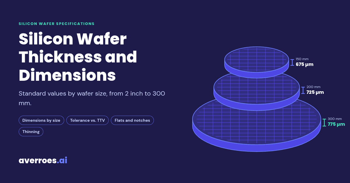
Surface preparation runs in 6 steps, from lapping to final qualification, finishing a 300 mm wafer at 775 µm thick with total thickness variation under 1 µm.
Polishing combines chemistry and mechanics: the slurry softens the surface while the pad shears it away, removing damage without adding new stress.
Each polishing step can create its own defect class: scratches and haze at polish, residue and water marks at cleaning, roll-off at the edge.
The polished surface sets the noise floor for inspection. Haze and residue raise the background every later laser scan must see through.
What Is Wafer Polishing and Why Does It Matter?
Wafer polishing is the chemical and mechanical surface preparation that removes the damage left by slicing and shaping and delivers the flatness and smoothness a fab’s lithography and deposition steps require. It matters for three reasons. Site flatness controls lithography focus across each exposure field. Surface roughness controls film quality and epitaxial growth. And the surface condition sets the baseline every inspection after it reads against: a hazy or residue-covered wafer hides the defects that matter.
Wafer surface preparation: 6 steps
Step
What Happens
Spec It Sets
Defect It Can Create
1. Lap or grind
Flatten both faces
Thickness, TTV
Residual damage, scratches
2. Etch
Dissolve damaged layer
Damage-free surface
Etch pits, stains
3. Double-side polish
Polish both faces at once
Flatness, nanotopography
Scratches, edge roll-off
4. Final polish
Finish the device face
Roughness, epi-ready surface
Micro-scratches, haze
5. Clean
RCA wet sequence
Particle and metal limits
Residue, water marks
6. Qualify
Scan, measure, sort
LPD count, haze level
Handling scratches
The diagram makes one point: every step that improves the surface can also damage it, and most polishing defects are only seen at final qualification, after the step that created them.
The Wafer Polishing Process, Step by Step
Wafer surface preparation runs in 6 steps. It is the back half of the wafer manufacturing stage, picking up where slicing and edge profiling leave off in the full sequence of how silicon wafers are made. Each step below follows the same pattern: what happens, the specification it sets, the defect it risks, and how that defect is caught.
1. Lap or Double-Disk Grind
Lapping is a mechanical flattening step that grinds both faces of a sliced wafer parallel, using an abrasive slurry between two counter-rotating plates. Many 300 mm lines use double-disk grinding instead, which does the same job with fixed-abrasive wheels. The difference from polishing is the goal: lapping removes stock to set geometry, while polishing refines the surface itself. Lapping takes out most of the saw damage and waviness and brings the wafer close to its final thickness.
Spec it sets: thickness, total thickness variation (TTV) and parallelism, measured per SEMI MF1530.
Defect risk: residual subsurface damage and scratches from oversized abrasive particles.
How it is caught: noncontact geometry tools that map thickness and flatness across the full wafer.
2. Etch Away Mechanical Damage
Wafer etching is a chemical step that dissolves the damaged layer left by slicing and lapping, without touching the geometry those steps set. Acid mixtures etch fast and leave a smoother surface. Alkaline solutions etch more uniformly and hold flatness better. Removing the damaged silicon also relieves the stress it carried, which protects the wafer from warping or cracking in later thermal steps.
Spec it sets: a damage-free surface while holding the flatness set at lapping.
Defect risk: etch pits, stains and flatness loss from uneven etch rates.
How it is caught: visual review under high-intensity light and haze measurement.
3. Double-Side Polish (DSP)
Double-side polishing is the chemical mechanical step that polishes both faces of a wafer at once, with the wafer held in a carrier between two rotating polyurethane pads flooded with colloidal silica slurry. The mechanism is the combination: the slurry’s alkaline chemistry softens the top molecular layers of silicon, and the pad’s mechanical action shears the softened material away. Neither alone produces a damage-free surface. Chemistry without mechanics stops removing material; mechanics without chemistry scratches.
Polishing both faces in one step is what sets global and site flatness, because material leaves both sides symmetrically and the wafer cannot bow toward one freshly polished face. Single-side polishing, used on smaller diameters and for the final finish, targets one face only.
Spec it sets: global flatness, site flatness and nanotopography.
Defect risk: scratches from agglomerated slurry particles and edge roll-off, where the pad over-polishes the wafer rim.
How it is caught: flatness and nanotopography metrology specified under SEMI M49 and SEMI M43.
The schematic shows why DSP controls flatness: the wafer floats in its carrier and both faces lose material at the same rate.
4. Final Single-Side Polish
The final polish is a short, soft-pad chemical mechanical step that finishes the device face of the wafer to its shipping condition. It removes very little material. Its job is surface quality: microroughness at the ångström scale, measured per SEMI M40, and a surface free of the fine scratches DSP can leave. A wafer finished to this grade and cleaned for epitaxial growth without further preparation is sold as epi-ready.
Spec it sets: final microroughness and the epi-ready surface condition.
Defect risk: micro-scratches and haze, a uniform light-scattering texture left by slurry chemistry or pad wear.
How it is caught: the haze channel of a laser scanner and microroughness measurement per SEMI M40.
5. Post-Polish Clean
Post-polish cleaning is the wet chemical sequence that removes slurry residue, particles and metals before the wafer is inspected. Most lines run a variant of the RCA clean: SC-1, a mix of ammonia and hydrogen peroxide, lifts particles and organics, and SC-2, a mix of hydrochloric acid and hydrogen peroxide, removes metals. SC-1 also etches the surface very slightly, which can open crystal originated particles from ingot growth into visible surface pits. This is where silicon ingot defects first appear on a scanner, even though polishing did not create them.
Spec it sets: particle count and surface metal limits.
Defect risk: remaining slurry residue, water marks from incomplete drying, and recontamination.
How it is caught: laser scanning for particles and total reflection X-ray fluorescence (TXRF) for surface metals.
6. Qualify the Surface
Surface qualification is the gate where every polished wafer is scanned, measured and sorted against its purchase specification before packing. Three tool types run here. Laser scanners (scanning surface inspection systems), specified under SEMI M52, sweep the surface and count and size light point defects (LPDs) while the haze channel maps background scattering. Geometry tools, specified under SEMI M49, confirm flatness and nanotopography. Macro and edge tools image the wafer at lower magnification for scratches, stains and rim defects.
The limit of this gate is what a scanner reports: light scattering, not defect identity. A real scratch fragment, a slurry residue spot and an opened crystal pit can return similar signals, so the count alone cannot say whether the surface preparation line has a problem. AI defect detection on the scanner and macro images sorts those detections into defect classes, so qualification decisions rest on what the defects are, not just how many light points scattered.
Spec it sets: final LPD count, haze level and the pass or fail against the purchase specification.
Defect risk: handling scratches added between final polish and packing.
How it is caught: this step is the catch, for every defect the earlier steps created.
What Surface Specifications Does Polishing Set?
Polishing sets the surface specifications of a prime wafer: site flatness, nanotopography and microroughness, each with its own SEMI measurement method, on top of the particle and haze limits set at cleaning and qualification. SEMI M1 defines a prime wafer as having at least one chem-mechanically polished surface, which makes polishing the step that decides whether a wafer is prime at all.
Specification
What It Measures
Why It Matters Downstream
Standard or Method
Site flatness (SFQR)
Flatness within each exposure-sized site
Focus error within a single die
SEMI M49, SEMI MF1530
Nanotopography
Short-wavelength height variation
Film thickness variation after fab CMP
SEMI M43
Microroughness
Surface texture at the ångström scale
Gate oxide quality, epitaxy
SEMI M40
Haze
Background light scattering
Noise floor for every laser scan
Laser scanner haze channel
Edge roll-off
Thickness drop at the wafer rim
Unusable die sites at the edge
Edge profile metrology
LPD count
Light point defects above a size threshold
Incoming qualification pass or fail
Laser scanner, per SEMI M52
The reference methods are anchors, not limits. The binding numbers live in each purchase specification built on SEMI M1, and they tighten with every technology generation. Dimensional and electrical specifications, including diameter, thickness, resistivity and crystal orientation, are set earlier in wafering and belong to the wafer specification itself rather than to polishing. Flatness connects to the wafer’s shape as a whole: see wafer bow and warp measurement for how bow and warp are measured and where their limits come from.
Flatness carries straight into yield. Poor site flatness becomes focus error inside a single exposure field, and nanotopography beyond spec becomes film thickness variation after the first chemical mechanical planarization in the fab.
What Defects Can Polishing Create?
Polishing defects are the scratches, haze, residue and edge flaws introduced during surface preparation, distinct from the saw damage created at slicing and the crystal defects grown into the ingot. Most are created at one step and only detected at final qualification.
Defect
Created at Step
Detected By
Downstream Risk at the Fab
Scratches
3. DSP, 4. Final polish, handling
Laser scanner, macro inspection
Pattern defects across every die the scratch crosses
Haze
4. Final polish
Laser scanner haze channel
A higher noise floor for every later inspection
Slurry residue
3. DSP to 5. Clean
Laser scanner
Counted as particles, blocks deposition locally
Water marks
5. Clean
Laser scanner, macro inspection
Local oxide and wetting variation
Particles
5. Clean to 6. Qualify
Laser scanner
Killer defects and a noisy inspection baseline
Edge roll-off
3. DSP
Edge profile metrology
Lost die sites at the wafer rim
Three relationships decide how much these defects cost. A scratch is a line defect, so it crosses every die in its path rather than one. Haze is not a killer defect itself, but it raises the scattering background that every later laser scan must see through, which hides small real defects. And edge roll-off removes usable area exactly where die already yield worst. The back surface carries its own risks after polishing, since a backside particle tilts the wafer on the lithography chuck: see inspecting wafer surfaces after polishing for the tools and failure modes.
Crystal originated particles follow a different path. They are grown in at ingot pulling, opened by the SC-1 clean, and counted by the scanner as if polishing had created them, which is exactly the ambiguity classification exists to resolve.
Substrate Polishing vs In-Fab CMP
Substrate polishing is a one-time surface preparation at the wafer supplier; chemical mechanical planarization (CMP) in the fab is a repeated between-layer step that flattens each deposited film during wafer fabrication. The chemistry is related. The job is different. Substrate polishing finishes a blank silicon surface once, to geometry and roughness targets. Fab CMP planarizes patterned oxide, metal and polysilicon layers, and at advanced nodes it runs dozens of times per wafer, each pass with its own slurry, pad and endpoint control.
The two meet at incoming qualification: the flatness and nanotopography the supplier’s polish delivered set the starting point every fab CMP pass planarizes from. In-fab CMP and its inspection belong to the wafer fabrication stage of the lifecycle, where lithography, etch, deposition and CMP cycle until the device is built.
Where AI Inspection Fits After Polishing
Post-polish surface qualification decides whether a wafer ships, and AI defect classification sorts what the laser scanner and macro tools detect into real defect classes and nuisance, without new inspection hardware. It matters at two gates. At the wafer supplier, final qualification holds or ships wafers on LPD counts that mix scratches, residue and opened crystal pits. At the fab, incoming qualification rescans the same wafers on its own tools and inherits the same ambiguity.
In both places the polished surface is the baseline being measured, so separating a process signal, such as a recurring scratch signature from a worn pad, from nuisance counts is what turns inspection data into a correction at the polishing line.
Averroes.ai runs AI visual inspection for semiconductor manufacturing as an overlay on the laser scanners and macro tools a supplier or fab already owns. It trains classification models from 20 to 40 labeled images per defect class, with no code, and deploys on premise so wafer image data stays inside the customer environment. It augments the installed qualification tools; it does not replace them.
Frequently Asked Questions
What is the wafer polishing process?
The wafer polishing process is the 6-step surface preparation sequence at a wafer supplier: lapping or grinding, chemical etching, double-side polishing, final single-side polishing, wet cleaning and surface qualification. Together the steps remove slicing damage and deliver the flatness, nanotopography and roughness a prime wafer must meet under SEMI M1.
What are the three types of polishing?
Wafer surface preparation uses three removal mechanisms: mechanical lapping, which grinds stock away with abrasives to set geometry; chemical etching, which dissolves damaged silicon without contact; and chemical mechanical polishing, which combines a softening slurry with pad pressure to produce a damage-free mirror finish. Production lines run all three in sequence.
How smooth is a polished silicon wafer?
A final-polished silicon wafer is smooth at the ångström scale, meaning its surface texture is measured in fractions of a nanometer. Microroughness is measured per SEMI M40, and the binding limit is set in each purchase specification. At that scale the surface is flat enough for gate oxides and epitaxial layers to grow uniformly.
What is the difference between lapping and polishing?
Lapping is mechanical stock removal that sets geometry: it grinds both faces parallel and brings the wafer to thickness, leaving a matte, damaged surface. Polishing is chemical mechanical finishing that sets surface quality: it removes little material but delivers the mirror finish, flatness and roughness the device face needs. Lapping always comes first.
What does epi-ready mean?
Epi-ready describes a polished wafer whose device face is finished and cleaned to a grade suitable for epitaxial growth without further surface preparation at the fab. The term is a surface condition, not a wafer type: an epi-ready wafer still meets its prime specification, with roughness and cleanliness controlled tightly enough to seed a defect-free epitaxial layer.
Is wafer polishing the same as CMP?
No. Wafer polishing at the supplier and chemical mechanical planarization (CMP) in the fab share the same slurry-and-pad chemistry but do different jobs. Substrate polishing finishes a blank wafer surface once, before shipment. Fab CMP planarizes patterned device layers between process steps and repeats dozens of times per wafer at advanced nodes.







Wafer polishing is the surface preparation sequence that turns a sliced, etched silicon wafer into a mirror-finish substrate flat enough for lithography. Wafers are lapped or ground flat, chemically etched to remove damage, polished on both sides with a chemical mechanical process, given a final single-side polish, then cleaned and inspected. The finished surface must meet the flatness, nanotopography and roughness limits of SEMI M1 before the wafer ships.
Surface preparation closes Stage 02 of the 12-stage semiconductor manufacturing process. This guide from Averroes.ai, an AI visual inspection platform for manufacturers, maps each step to the surface specification it sets and the defect it can create.
Key Notes
What Is Wafer Polishing and Why Does It Matter?
Wafer polishing is the chemical and mechanical surface preparation that removes the damage left by slicing and shaping and delivers the flatness and smoothness a fab’s lithography and deposition steps require. It matters for three reasons. Site flatness controls lithography focus across each exposure field. Surface roughness controls film quality and epitaxial growth. And the surface condition sets the baseline every inspection after it reads against: a hazy or residue-covered wafer hides the defects that matter.
Wafer surface preparation: 6 steps
The diagram makes one point: every step that improves the surface can also damage it, and most polishing defects are only seen at final qualification, after the step that created them.
The Wafer Polishing Process, Step by Step
Wafer surface preparation runs in 6 steps. It is the back half of the wafer manufacturing stage, picking up where slicing and edge profiling leave off in the full sequence of how silicon wafers are made. Each step below follows the same pattern: what happens, the specification it sets, the defect it risks, and how that defect is caught.
1. Lap or Double-Disk Grind
Lapping is a mechanical flattening step that grinds both faces of a sliced wafer parallel, using an abrasive slurry between two counter-rotating plates. Many 300 mm lines use double-disk grinding instead, which does the same job with fixed-abrasive wheels. The difference from polishing is the goal: lapping removes stock to set geometry, while polishing refines the surface itself. Lapping takes out most of the saw damage and waviness and brings the wafer close to its final thickness.
2. Etch Away Mechanical Damage
Wafer etching is a chemical step that dissolves the damaged layer left by slicing and lapping, without touching the geometry those steps set. Acid mixtures etch fast and leave a smoother surface. Alkaline solutions etch more uniformly and hold flatness better. Removing the damaged silicon also relieves the stress it carried, which protects the wafer from warping or cracking in later thermal steps.
3. Double-Side Polish (DSP)
Double-side polishing is the chemical mechanical step that polishes both faces of a wafer at once, with the wafer held in a carrier between two rotating polyurethane pads flooded with colloidal silica slurry. The mechanism is the combination: the slurry’s alkaline chemistry softens the top molecular layers of silicon, and the pad’s mechanical action shears the softened material away. Neither alone produces a damage-free surface. Chemistry without mechanics stops removing material; mechanics without chemistry scratches.
Polishing both faces in one step is what sets global and site flatness, because material leaves both sides symmetrically and the wafer cannot bow toward one freshly polished face. Single-side polishing, used on smaller diameters and for the final finish, targets one face only.
The schematic shows why DSP controls flatness: the wafer floats in its carrier and both faces lose material at the same rate.
4. Final Single-Side Polish
The final polish is a short, soft-pad chemical mechanical step that finishes the device face of the wafer to its shipping condition. It removes very little material. Its job is surface quality: microroughness at the ångström scale, measured per SEMI M40, and a surface free of the fine scratches DSP can leave. A wafer finished to this grade and cleaned for epitaxial growth without further preparation is sold as epi-ready.
5. Post-Polish Clean
Post-polish cleaning is the wet chemical sequence that removes slurry residue, particles and metals before the wafer is inspected. Most lines run a variant of the RCA clean: SC-1, a mix of ammonia and hydrogen peroxide, lifts particles and organics, and SC-2, a mix of hydrochloric acid and hydrogen peroxide, removes metals. SC-1 also etches the surface very slightly, which can open crystal originated particles from ingot growth into visible surface pits. This is where silicon ingot defects first appear on a scanner, even though polishing did not create them.
6. Qualify the Surface
Surface qualification is the gate where every polished wafer is scanned, measured and sorted against its purchase specification before packing. Three tool types run here. Laser scanners (scanning surface inspection systems), specified under SEMI M52, sweep the surface and count and size light point defects (LPDs) while the haze channel maps background scattering. Geometry tools, specified under SEMI M49, confirm flatness and nanotopography. Macro and edge tools image the wafer at lower magnification for scratches, stains and rim defects.
The limit of this gate is what a scanner reports: light scattering, not defect identity. A real scratch fragment, a slurry residue spot and an opened crystal pit can return similar signals, so the count alone cannot say whether the surface preparation line has a problem. AI defect detection on the scanner and macro images sorts those detections into defect classes, so qualification decisions rest on what the defects are, not just how many light points scattered.
What Surface Specifications Does Polishing Set?
Polishing sets the surface specifications of a prime wafer: site flatness, nanotopography and microroughness, each with its own SEMI measurement method, on top of the particle and haze limits set at cleaning and qualification. SEMI M1 defines a prime wafer as having at least one chem-mechanically polished surface, which makes polishing the step that decides whether a wafer is prime at all.
The reference methods are anchors, not limits. The binding numbers live in each purchase specification built on SEMI M1, and they tighten with every technology generation. Dimensional and electrical specifications, including diameter, thickness, resistivity and crystal orientation, are set earlier in wafering and belong to the wafer specification itself rather than to polishing. Flatness connects to the wafer’s shape as a whole: see wafer bow and warp measurement for how bow and warp are measured and where their limits come from.
Flatness carries straight into yield. Poor site flatness becomes focus error inside a single exposure field, and nanotopography beyond spec becomes film thickness variation after the first chemical mechanical planarization in the fab.
What Defects Can Polishing Create?
Polishing defects are the scratches, haze, residue and edge flaws introduced during surface preparation, distinct from the saw damage created at slicing and the crystal defects grown into the ingot. Most are created at one step and only detected at final qualification.
Three relationships decide how much these defects cost. A scratch is a line defect, so it crosses every die in its path rather than one. Haze is not a killer defect itself, but it raises the scattering background that every later laser scan must see through, which hides small real defects. And edge roll-off removes usable area exactly where die already yield worst. The back surface carries its own risks after polishing, since a backside particle tilts the wafer on the lithography chuck: see inspecting wafer surfaces after polishing for the tools and failure modes.
Crystal originated particles follow a different path. They are grown in at ingot pulling, opened by the SC-1 clean, and counted by the scanner as if polishing had created them, which is exactly the ambiguity classification exists to resolve.
Substrate Polishing vs In-Fab CMP
Substrate polishing is a one-time surface preparation at the wafer supplier; chemical mechanical planarization (CMP) in the fab is a repeated between-layer step that flattens each deposited film during wafer fabrication. The chemistry is related. The job is different. Substrate polishing finishes a blank silicon surface once, to geometry and roughness targets. Fab CMP planarizes patterned oxide, metal and polysilicon layers, and at advanced nodes it runs dozens of times per wafer, each pass with its own slurry, pad and endpoint control.
The two meet at incoming qualification: the flatness and nanotopography the supplier’s polish delivered set the starting point every fab CMP pass planarizes from. In-fab CMP and its inspection belong to the wafer fabrication stage of the lifecycle, where lithography, etch, deposition and CMP cycle until the device is built.
Where AI Inspection Fits After Polishing
Post-polish surface qualification decides whether a wafer ships, and AI defect classification sorts what the laser scanner and macro tools detect into real defect classes and nuisance, without new inspection hardware. It matters at two gates. At the wafer supplier, final qualification holds or ships wafers on LPD counts that mix scratches, residue and opened crystal pits. At the fab, incoming qualification rescans the same wafers on its own tools and inherits the same ambiguity.
In both places the polished surface is the baseline being measured, so separating a process signal, such as a recurring scratch signature from a worn pad, from nuisance counts is what turns inspection data into a correction at the polishing line.
Averroes.ai runs AI visual inspection for semiconductor manufacturing as an overlay on the laser scanners and macro tools a supplier or fab already owns. It trains classification models from 20 to 40 labeled images per defect class, with no code, and deploys on premise so wafer image data stays inside the customer environment. It augments the installed qualification tools; it does not replace them.
Frequently Asked Questions
What is the wafer polishing process?
The wafer polishing process is the 6-step surface preparation sequence at a wafer supplier: lapping or grinding, chemical etching, double-side polishing, final single-side polishing, wet cleaning and surface qualification. Together the steps remove slicing damage and deliver the flatness, nanotopography and roughness a prime wafer must meet under SEMI M1.
What are the three types of polishing?
Wafer surface preparation uses three removal mechanisms: mechanical lapping, which grinds stock away with abrasives to set geometry; chemical etching, which dissolves damaged silicon without contact; and chemical mechanical polishing, which combines a softening slurry with pad pressure to produce a damage-free mirror finish. Production lines run all three in sequence.
How smooth is a polished silicon wafer?
A final-polished silicon wafer is smooth at the ångström scale, meaning its surface texture is measured in fractions of a nanometer. Microroughness is measured per SEMI M40, and the binding limit is set in each purchase specification. At that scale the surface is flat enough for gate oxides and epitaxial layers to grow uniformly.
What is the difference between lapping and polishing?
Lapping is mechanical stock removal that sets geometry: it grinds both faces parallel and brings the wafer to thickness, leaving a matte, damaged surface. Polishing is chemical mechanical finishing that sets surface quality: it removes little material but delivers the mirror finish, flatness and roughness the device face needs. Lapping always comes first.
What does epi-ready mean?
Epi-ready describes a polished wafer whose device face is finished and cleaned to a grade suitable for epitaxial growth without further surface preparation at the fab. The term is a surface condition, not a wafer type: an epi-ready wafer still meets its prime specification, with roughness and cleanliness controlled tightly enough to seed a defect-free epitaxial layer.
Is wafer polishing the same as CMP?
No. Wafer polishing at the supplier and chemical mechanical planarization (CMP) in the fab share the same slurry-and-pad chemistry but do different jobs. Substrate polishing finishes a blank wafer surface once, before shipment. Fab CMP planarizes patterned device layers between process steps and repeats dozens of times per wafer at advanced nodes.