Silicon Wafer Thickness and Dimensions: Standard Values by Wafer Size
Averroes
Oct 21, 2026
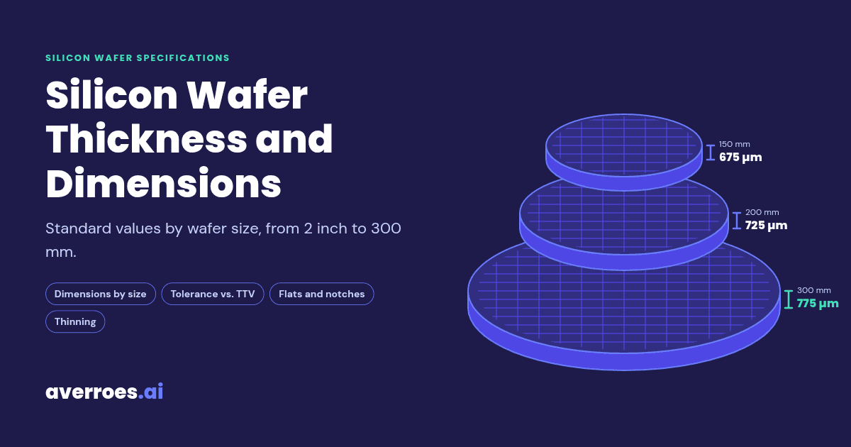
Standard silicon wafer thickness rises with diameter, from 279 µm for a 2-inch wafer to 775 µm for a 300 mm wafer, with 725 µm at 200 mm and 675 µm at 150 mm. Larger wafers are thicker so they stay rigid through handling and processing. Thickness tolerance is typically about ±20 µm, and many finished wafers are thinned to 100 to 300 µm before packaging.
This reference from Averroes.ai, an AI visual inspection platform for manufacturers, covers every standard wafer size, the specs that govern thickness, and how thickness changes after the wafer manufacturing stage.
Key Notes
A 300 mm silicon wafer is 775 µm thick and weighs about 128 g.
Thickness tolerance and TTV are different specs: tolerance is deviation from nominal, TTV is variation within one wafer, under 1 µm on 300 mm prime wafers.
Wafers 200 mm and larger use a notch, while 150 mm and smaller use flats.
Wafer thickness falls through the process, from 775 µm in the fab to below 50 µm for some advanced packaging die.
Silicon Wafer Dimensions by Wafer Size
Silicon wafer dimensions are the standardized diameter, thickness, tolerance and orientation marks set for each wafer size, defined for polished wafers in SEMI M1. Every standard size pairs one diameter with one or two nominal thicknesses, so tools and carriers built for that size can handle any compliant wafer.
Silicon wafer dimensions by wafer size
Wafer Size
Nominal Thickness
Thickness in Mils
Orientation Mark
Primary Flat Length
Approx. Weight
50.8 mm (2 in)
279 µm
11.0
Flats
15.88 mm
1.3 g
76.2 mm (3 in)
381 µm
15.0
Flats
22.22 mm
4.1 g
100 mm (4 in)
525 µm (or 625 µm)
20.7
Flats
32.5 mm
9.6 g
125 mm (5 in)
625 µm
24.6
Flats
42.5 mm
17.9 g
150 mm (6 in)
675 µm (or 625 µm)
26.6
Flats
57.5 mm
27.8 g
200 mm (8 in)
725 µm
28.5
Notch
None
53.1 g
300 mm (12 in)
775 µm
30.5
Notch
None
127.6 g
450 mm (18 in)
925 µm
36.4
Developmental (SEMI M76)
None
342.8 g
Thickness values follow the SEMI standard thickness table published by Addison Engineering. Flat lengths follow standard wafer dimension drawings, which list a thickness tolerance of ±20 µm for 200 mm and 300 mm wafers. Weights are calculated, not measured (see the FAQ for the formula).
Two sizes have two common thicknesses. 100 mm wafers ship at 525 µm or 625 µm, and 150 mm wafers at 675 µm or 625 µm, depending on the process and the supplier.
Published figures for these values don’t always agree, so confirm the nominal thickness and tolerance against SEMI M1 and the supplier datasheet before writing a purchase spec. The 450 mm row reflects a developmental specification: 450 mm wafers never reached volume production.
The graphic shows the pattern in the table: each step up in diameter adds 50 to 150 µm of thickness, while wafer weight grows far faster, from about 53 g at 200 mm to about 128 g at 300 mm.
Why Does Wafer Thickness Increase With Diameter?
Wafer thickness increases with diameter because a larger disc sags, bows and breaks more easily, so it needs more material to stay rigid. For a thin disc supported at its edge, gravitational sag scales roughly with the fourth power of the radius divided by the square of the thickness. Doubling the diameter at the same thickness would make a wafer sag about 16 times more.
That stiffness matters at four points in the process:
Handling. Robots, end effectors and carriers support the wafer at a few points. A wafer that flexes too much contacts the carrier, scratches or breaks.
Lithography chucking. The chuck pulls the wafer flat by vacuum or electrostatic force. Bow and warp beyond the chuck’s tolerance leave the surface out of focus across the exposure field. See wafer bow and warp measurement for how these are measured.
Thermal processing. Furnaces and rapid thermal tools heat the wafer unevenly at the edge. A thin, large wafer is more likely to slip or warp under that stress.
Mechanical breakage. Thicker wafers survive the small impacts of transfer and cassette loading that would crack a thinner one.
Thicker is not free. Every extra micron of thickness is silicon a fab pays for and, for many devices, silicon that is ground away later at backgrinding. Each standard thickness is a compromise: the thinnest wafer that still handles, chucks and survives thermal steps reliably at that diameter.
Thickness Tolerance vs. Total Thickness Variation (TTV)
Thickness tolerance is how far a wafer’s thickness may deviate from its nominal value, while total thickness variation (TTV) is the difference between the thickest and thinnest points on a single wafer. Datasheets list both, and they answer different questions: tolerance says whether the wafer is the right thickness, TTV says whether it is flat enough to pattern.
Thickness Tolerance
Total Thickness Variation (TTV)
What it measures
Deviation of center thickness from nominal
Maximum minus minimum thickness across one wafer
Scope
Wafer to wafer, across a lot
Within a single wafer
Typical 300 mm prime value
±20 to ±25 µm
Under 1 µm
What it affects
Tool handling, wafer stacking in carriers, backgrind targets
Lithography focus, CMP uniformity
What sets it
Slicing and total material removal
Lapping or grinding, then polishing
Test method
SEMI MF533
SEMI MF1530
The difference is large in practice. One supplier’s standard 300 mm prime wafer is specified at 775 ±25 µm thick with TTV of 0.9 µm or less, so wafers in the same lot can differ by 50 µm in thickness while each one stays flat to under a micron.
TTV is where wafer grade shows. In one supplier’s published 150 mm specification, Prime A wafers carry TTV under 2 to 5 µm, while test-grade wafers allow up to 15 µm.
TTV is set during wafer manufacturing, mostly at lapping or double-disk grinding and then at polishing. Slicing sets the rough thickness, and every later removal step tightens the variation. See how silicon wafers are made for each step.
The diagram’s point: a lot can pass tolerance and still fail TTV, because tolerance looks across wafers and TTV looks inside each one.
Wafer Flats and Notches
Flats and notches are features ground into a wafer’s edge to mark crystal orientation, and on smaller wafers the secondary flat also indicates conductivity type. Every downstream tool uses the mark to rotate the wafer to the same position before it processes or measures it.
150 mm and smaller wafers use flats. The primary flat, the longest one, is aligned to a specific crystal plane. Its length is standardized per diameter, from 15.88 mm on a 2-inch wafer to 57.5 mm on a 150 mm wafer. A shorter secondary flat, such as 18.0 mm on a 100 mm wafer or 37.5 mm on a 150 mm wafer, sits at a set angle from the primary, and that angle encodes the wafer’s type and orientation.
200 mm and 300 mm wafers use a notch. A single small V-shaped notch marks orientation and wastes far less of the wafer’s edge than a flat. A notch does not show the doping type, so type and orientation are read from the laser-marked wafer ID and the lot paperwork instead.
Flat length is measured per SEMI MF671 and notch dimensions per SEMI MF1152.
How Wafer Thickness Changes Through the Process
Wafer thickness is not fixed: a wafer is cut thicker than its final value, polished to nominal thickness for fabrication, then often thinned by backgrinding before packaging. A 300 mm wafer passes through four thickness stages:
As cut. The wire saw leaves each slice thicker than nominal, because lapping, etching and polishing will remove material from both faces.
Polished to nominal, 775 µm. The wafer holds this thickness through the whole front-end flow, often hundreds of process steps, because that is when it needs full rigidity.
Backgrinding to about 100 to 300 µm. After fabrication, the back of the wafer is ground away so the finished die fits a thinner package and sheds heat better. The final value depends on the application.
Below 50 µm for some advanced packaging die. Stacked memory and 3D integration push die thinner still. At this thickness, wafers are handled on tape or bonded to a carrier.
The opposite case exists too. Thick silicon wafers serve as carrier substrates, giving mechanical support to thin device wafers during deep etching or bonding.
Thinner wafers change the defect picture at wafer dicing. Below 50 µm, edge quality becomes a reliability question, not a cosmetic one. A die edge crack that passes visual inspection can survive final test and fail after thermal cycling in the field. Blade and laser dicing also leave normal artefacts along every edge, so telling an acceptable kerf signature from a real chip is a classification problem, not a threshold setting.
Averroes.ai addresses that problem as an overlay on the dicing inspection tools a line already runs. Its models learn the line’s own normal edge for each blade, material and recipe from 20 to 40 labeled images per defect class, then flag real cracks and chips.
Thin Die, Fragile Edges?
See how AI defect detection handles thin-die edge inspection
How Is Wafer Thickness Measured?
Wafer thickness is measured with noncontact capacitive or optical gauges that scan the full wafer and report thickness, TTV, bow and warp together. A single scan collects thousands of points, so one measurement covers every geometry spec on the datasheet.
Method
How It Works
Typical Use
Capacitive gauge
Paired sensors above and below the wafer measure the gap to each surface
Incoming and outgoing wafer geometry, bare wafers
Optical interferometry
Light reflected from both surfaces, or through the silicon, gives thickness directly
Spot checks and lab work, less common in production
The test methods are standardized. SEMI MF533 covers thickness and thickness variation, and SEMI MF1530 covers flatness, thickness and TTV by automated noncontact scanning.
Thin wafers need different support. A thin, large wafer sags under its own weight on standard three-point supports, which distorts bow and warp readings. SEMI 3D12 provides an alternative method for low-stiffness wafers of 300 mm and larger at 775 µm or thinner.
During backgrinding, optical thickness measurement runs in line and tells the grinder when to stop, so the wafer reaches its target without a separate measurement step.
Frequently Asked Questions
How thick is a 300 mm silicon wafer?
A 300 mm silicon wafer is 775 µm thick nominally, about 30.5 mils, with a typical tolerance of ±20 to ±25 µm. Prime 300 mm wafers hold total thickness variation under 1 µm. The wafer keeps this thickness through front-end fabrication and is often thinned by backgrinding afterward.
How much does a silicon wafer weigh?
A 300 mm silicon wafer weighs about 128 g, a 200 mm wafer about 53 g and a 150 mm wafer about 28 g. Weight equals π × radius² × thickness × 2.33 g/cm³, the density of silicon. For a 300 mm wafer: π × (15 cm)² × 0.0775 cm × 2.33 g/cm³ ≈ 127.6 g.
What is silicon wafer thickness in mils?
One mil equals 25.4 µm, so a 775 µm 300 mm wafer is about 30.5 mils, a 725 µm 200 mm wafer about 28.5 mils, and a 525 µm 100 mm wafer about 20.7 mils. Older datasheets for small wafers often list thickness in mils, such as 11 mils for a 2-inch wafer.
Why are wafers thinned before packaging?
Wafers are thinned by backgrinding after fabrication so the finished die fits thinner packages, dissipates heat better and can be stacked for 3D integration. Thinning happens only after front-end processing because the wafer needs its full thickness to stay rigid through hundreds of fab steps.
How thin can a silicon wafer be?
Backgrinding commonly takes wafers to about 100 to 300 µm, depending on the application. Some advanced packaging die go below 50 µm. At that thickness a wafer can no longer support itself, so it is handled on tape or bonded to a carrier wafer, and edge cracks at dicing become a reliability risk.
Are solar wafers thinner than semiconductor wafers?
Yes, solar wafers are generally cut thinner than prime semiconductor wafers and are usually square or pseudo-square rather than round. Their thickness is set by cost per watt and cell design rather than by fab handling. Values vary by cell technology and supplier, so check the specific datasheet.









Standard silicon wafer thickness rises with diameter, from 279 µm for a 2-inch wafer to 775 µm for a 300 mm wafer, with 725 µm at 200 mm and 675 µm at 150 mm. Larger wafers are thicker so they stay rigid through handling and processing. Thickness tolerance is typically about ±20 µm, and many finished wafers are thinned to 100 to 300 µm before packaging.
This reference from Averroes.ai, an AI visual inspection platform for manufacturers, covers every standard wafer size, the specs that govern thickness, and how thickness changes after the wafer manufacturing stage.
Key Notes
Silicon Wafer Dimensions by Wafer Size
Silicon wafer dimensions are the standardized diameter, thickness, tolerance and orientation marks set for each wafer size, defined for polished wafers in SEMI M1. Every standard size pairs one diameter with one or two nominal thicknesses, so tools and carriers built for that size can handle any compliant wafer.
Silicon wafer dimensions by wafer size
Thickness values follow the SEMI standard thickness table published by Addison Engineering. Flat lengths follow standard wafer dimension drawings, which list a thickness tolerance of ±20 µm for 200 mm and 300 mm wafers. Weights are calculated, not measured (see the FAQ for the formula).
Two sizes have two common thicknesses. 100 mm wafers ship at 525 µm or 625 µm, and 150 mm wafers at 675 µm or 625 µm, depending on the process and the supplier.
Published figures for these values don’t always agree, so confirm the nominal thickness and tolerance against SEMI M1 and the supplier datasheet before writing a purchase spec. The 450 mm row reflects a developmental specification: 450 mm wafers never reached volume production.
The graphic shows the pattern in the table: each step up in diameter adds 50 to 150 µm of thickness, while wafer weight grows far faster, from about 53 g at 200 mm to about 128 g at 300 mm.
Why Does Wafer Thickness Increase With Diameter?
Wafer thickness increases with diameter because a larger disc sags, bows and breaks more easily, so it needs more material to stay rigid. For a thin disc supported at its edge, gravitational sag scales roughly with the fourth power of the radius divided by the square of the thickness. Doubling the diameter at the same thickness would make a wafer sag about 16 times more.
That stiffness matters at four points in the process:
Thicker is not free. Every extra micron of thickness is silicon a fab pays for and, for many devices, silicon that is ground away later at backgrinding. Each standard thickness is a compromise: the thinnest wafer that still handles, chucks and survives thermal steps reliably at that diameter.
Thickness Tolerance vs. Total Thickness Variation (TTV)
Thickness tolerance is how far a wafer’s thickness may deviate from its nominal value, while total thickness variation (TTV) is the difference between the thickest and thinnest points on a single wafer. Datasheets list both, and they answer different questions: tolerance says whether the wafer is the right thickness, TTV says whether it is flat enough to pattern.
The difference is large in practice. One supplier’s standard 300 mm prime wafer is specified at 775 ±25 µm thick with TTV of 0.9 µm or less, so wafers in the same lot can differ by 50 µm in thickness while each one stays flat to under a micron.
TTV is where wafer grade shows. In one supplier’s published 150 mm specification, Prime A wafers carry TTV under 2 to 5 µm, while test-grade wafers allow up to 15 µm.
TTV is set during wafer manufacturing, mostly at lapping or double-disk grinding and then at polishing. Slicing sets the rough thickness, and every later removal step tightens the variation. See how silicon wafers are made for each step.
The diagram’s point: a lot can pass tolerance and still fail TTV, because tolerance looks across wafers and TTV looks inside each one.
Wafer Flats and Notches
Flats and notches are features ground into a wafer’s edge to mark crystal orientation, and on smaller wafers the secondary flat also indicates conductivity type. Every downstream tool uses the mark to rotate the wafer to the same position before it processes or measures it.
Flat length is measured per SEMI MF671 and notch dimensions per SEMI MF1152.
How Wafer Thickness Changes Through the Process
Wafer thickness is not fixed: a wafer is cut thicker than its final value, polished to nominal thickness for fabrication, then often thinned by backgrinding before packaging. A 300 mm wafer passes through four thickness stages:
The opposite case exists too. Thick silicon wafers serve as carrier substrates, giving mechanical support to thin device wafers during deep etching or bonding.
Thinner wafers change the defect picture at wafer dicing. Below 50 µm, edge quality becomes a reliability question, not a cosmetic one. A die edge crack that passes visual inspection can survive final test and fail after thermal cycling in the field. Blade and laser dicing also leave normal artefacts along every edge, so telling an acceptable kerf signature from a real chip is a classification problem, not a threshold setting.
Averroes.ai addresses that problem as an overlay on the dicing inspection tools a line already runs. Its models learn the line’s own normal edge for each blade, material and recipe from 20 to 40 labeled images per defect class, then flag real cracks and chips.
Thin Die, Fragile Edges?
See how AI defect detection handles thin-die edge inspection
How Is Wafer Thickness Measured?
Wafer thickness is measured with noncontact capacitive or optical gauges that scan the full wafer and report thickness, TTV, bow and warp together. A single scan collects thousands of points, so one measurement covers every geometry spec on the datasheet.
The test methods are standardized. SEMI MF533 covers thickness and thickness variation, and SEMI MF1530 covers flatness, thickness and TTV by automated noncontact scanning.
Thin wafers need different support. A thin, large wafer sags under its own weight on standard three-point supports, which distorts bow and warp readings. SEMI 3D12 provides an alternative method for low-stiffness wafers of 300 mm and larger at 775 µm or thinner.
During backgrinding, optical thickness measurement runs in line and tells the grinder when to stop, so the wafer reaches its target without a separate measurement step.
Frequently Asked Questions
How thick is a 300 mm silicon wafer?
A 300 mm silicon wafer is 775 µm thick nominally, about 30.5 mils, with a typical tolerance of ±20 to ±25 µm. Prime 300 mm wafers hold total thickness variation under 1 µm. The wafer keeps this thickness through front-end fabrication and is often thinned by backgrinding afterward.
How much does a silicon wafer weigh?
A 300 mm silicon wafer weighs about 128 g, a 200 mm wafer about 53 g and a 150 mm wafer about 28 g. Weight equals π × radius² × thickness × 2.33 g/cm³, the density of silicon. For a 300 mm wafer: π × (15 cm)² × 0.0775 cm × 2.33 g/cm³ ≈ 127.6 g.
What is silicon wafer thickness in mils?
One mil equals 25.4 µm, so a 775 µm 300 mm wafer is about 30.5 mils, a 725 µm 200 mm wafer about 28.5 mils, and a 525 µm 100 mm wafer about 20.7 mils. Older datasheets for small wafers often list thickness in mils, such as 11 mils for a 2-inch wafer.
Why are wafers thinned before packaging?
Wafers are thinned by backgrinding after fabrication so the finished die fits thinner packages, dissipates heat better and can be stacked for 3D integration. Thinning happens only after front-end processing because the wafer needs its full thickness to stay rigid through hundreds of fab steps.
How thin can a silicon wafer be?
Backgrinding commonly takes wafers to about 100 to 300 µm, depending on the application. Some advanced packaging die go below 50 µm. At that thickness a wafer can no longer support itself, so it is handled on tape or bonded to a carrier wafer, and edge cracks at dicing become a reliability risk.
Are solar wafers thinner than semiconductor wafers?
Yes, solar wafers are generally cut thinner than prime semiconductor wafers and are usually square or pseudo-square rather than round. Their thickness is set by cost per watt and cell design rather than by fab handling. Values vary by cell technology and supplier, so check the specific datasheet.