Overlay Metrology in Semiconductor Lithography: Tools, Targets and Error Sources
Averroes
Nov 02, 2026
Overlay metrology measures how accurately each new patterned layer sits on the layers beneath it, using dedicated targets printed in the scribe lines of a semiconductor wafer. It is measured after develop, on sampled fields and wafers, by image-based (IBO) or diffraction-based (DBO) methods, and its output feeds corrections back to the lithography scanner. At advanced nodes the whole overlay budget is a couple of nanometers, which makes it one of the tightest controlled parameters in the fab.
Overlay metrology runs inside Stage 03 of the 12-stage semiconductor manufacturing process, alongside the inspection gates that check the same wafers for defects. This guide from Averroes.ai, an AI visual inspection and virtual metrology platform for manufacturers, covers the targets, the two measurement families, where overlay error actually comes from, and how sampled measurements and predictions together keep a scanner corrected.
Key Notes
Alignment and overlay are different things: alignment is what the scanner does before exposure, overlay is what metrology measures after develop.
Overlay is measured on dedicated targets, by image-based (IBO) or diffraction-based (DBO) methods, not on the device pattern itself.
Overlay error comes from three directions: the scanner, the process steps that distort the marks, and the marks themselves.
Only a sampled fraction of fields and wafers is ever measured. The rest is corrected on model, which is where prediction earns its place.
What Overlay Metrology Is, and What It Is Not
Overlay is the registration error between a newly printed layer and the layer beneath it; overlay metrology is the measurement of that error on dedicated targets after develop. Three distinctions keep the term precise, and none of them is pedantry, because each names a different engineering activity.
Alignment is not overlay. Before exposure, the scanner aligns the wafer to marks from previous layers; that is an action the scanner takes, part of the photolithography process itself. Overlay is measured afterward, on the developed resist, and grades how well that alignment actually worked. The first is steering; the second is the scorecard.
Overlay is not CD. Both are metrology on the developed wafer, but they answer different questions: overlay asks whether the layer is where it should be, and critical dimension measurement asks whether the features are the right size.
Overlay metrology is not defect inspection. The same developed wafer also passes post-develop inspection, which checks whether the pattern is intact. The two run side by side and share one piece of economics: an overlay reject at the develop stage is still strippable, so a misregistered layer caught here costs a rework pass, not the wafer.
Three measurements on a developed wafer
Check
Question It Answers
Where Covered
Overlay metrology
Is the layer where it should be?
This page
CD metrology
Are the features the right size?
CD guide
Defect inspection
Is the pattern intact?
PDI guide
Overlay Targets
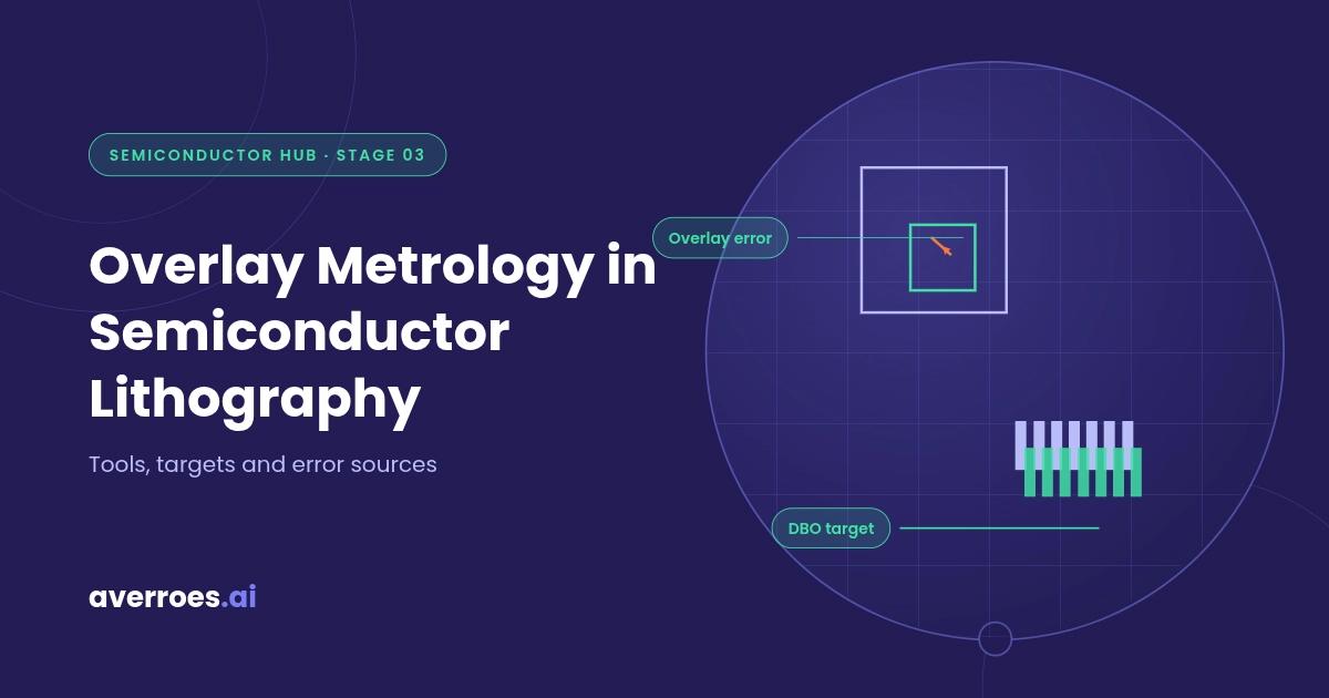
An overlay target is a measurable structure printed in two layers: one half by the previous layer and one half by the current one, so the offset between the halves is the overlay error. Targets live in the scribe lines between dies, where they can be built for measurability rather than function.
The classic imaged target is box-in-box overlay, an inner box printed by the current layer inside an outer box from the previous one, with frame-in-frame as its relative; the measured quantity is the centering of one on the other. AIM-style targets replace the boxes with segmented gratings arranged so one image yields overlay in both directions with better averaging. Diffraction-based targets are pairs of overlapping gratings printed with a deliberate, known offset called a programmed bias, which turns the overlay error into a measurable asymmetry.
Two realities shape target engineering. Scribe-line real estate shrinks as more measurements compete for it, which pushes targets smaller and multi-purpose. And the target is a proxy: it is not the device, and the offset between what the target reports and what the device experiences is a named error term, not a rounding detail. Target design is its own field for exactly these reasons.
The panel’s takeaway in one line: every target is two layers made to disagree measurably, and the disagreement is the number.
How Overlay Is Measured: IBO and DBO
Two method families dominate overlay measurement: image-based overlay images the target and measures the offset geometrically, and diffraction-based overlay reads it from the asymmetry of diffracted light.
The split in one line: IBO measures a picture, DBO measures a signal, and the choice between them is a precision-against-flexibility trade.
Image-Based Overlay (IBO)
Image based overlay acquires a brightfield microscope image of the target, box-in-box or AIM, and computes the offset between the two layers’ features edge to edge. Its strengths are directness and flexibility: the measurement is interpretable by eye, target shapes can vary, and recipe setup is comparatively simple. Its limits arrive with scale: at small features, low resist contrast and thick film stacks, the optical image carries less information than the measurement needs.
Diffraction-Based Overlay (DBO)
Diffraction based overlay illuminates a grating-pair target and reads the asymmetry between diffracted orders; with two pads at opposite programmed bias, the asymmetry converts directly into the overlay value. The method does not image the target at all, which is why it keeps precision and sensitivity where imaging runs out, and why it carries advanced-node overlay. The costs are its own: grating pads per measurement direction consume more scribe space, and performance depends on wavelength and recipe setup tuned per stack, because the signal rides on the films it passes through.
Choosing Between Them
The practical split follows from the physics: IBO where flexibility, interpretability and target variety matter, DBO where the budget demands its precision, and hybrid use on the same wafer is routine. The canonical treatment of both families and their mark design is Den Boef’s overlay metrology work, which remains the field’s reference.
Where Overlay Error Comes From
Overlay error is the sum of what the scanner contributed, what the process did to the wafer and its marks, and what the marks themselves fail to represent. Treating it as one number hides the fact that three different owners have to fix it.
Scanner and Stage
The scanner’s own contributions include stage positioning error, lens distortion across the exposure field, reticle and chuck effects, and the thermal terms, lens heating and wafer heating, that drift within a lot. These are the terms the correction loop exists to cancel, and the reason overlay error in lithography is modeled per field and per wafer rather than averaged away.
Process-Induced Distortion
Much of every overlay number is made outside lithography. Deposited films, etch and anneal stress the wafer and warp it; the marks move with the wafer they sit on. Planarization distorts marks directly: dishing on metal targets changes the very asymmetry that DBO measures, which is one of the quiet ways the polish described under post-CMP inspection reaches into metrology. And in wafer-to-wafer and die-to-die bonding, substrate distortion becomes its own overlay discipline, with hybrid metrology methods built for it.
Mark Asymmetry and Target Error
The target itself is the third source. A damaged, asymmetric or unrepresentative mark reads as overlay error that the devices never experienced: process steps can erode one side of a grating, fill a box unevenly, or leave the target behaving differently from the pattern it stands for. Separating mark error from real registration error is a standing part of recipe and target qualification.
The budget these sources share is unforgiving. At advanced nodes, overlay must be controlled below roughly 2 nm at three sigma, consuming less than 20 to 30 percent of the critical dimension error budget, per the Optica Publishing Group overlay literature; verify the exact figures against the source at publish. Within a budget that size, every one of the three sources above is material.
Sampling and the Correction Loop
Overlay measurements exist to be fed back: sampled fields on sampled wafers are measured, modeled, and turned into corrections the scanner applies to the next exposures.
Sampling is the first economic fact of overlay. Measurement time is throughput, so no fab measures every field on every wafer; a sampling plan selects a fraction of fields on a subset of wafers per lot. The measurements feed an overlay model that decomposes the error into inter-field terms, the grid across the wafer, and intra-field terms, the signature within each exposure, and the model’s coefficients become correctables the scanner can act on.
Run to run control is the loop that applies them: overlay measured on one lot corrects the scanner for the next, continuously, so slow drifts in the scanner and the process are cancelled before they grow. Excursions follow a different path, triggering holds and root-cause work rather than routine correction, but the steady state of modern lithography is this loop running quietly on sampled data.
The loop’s takeaway is also its gap: everything it corrects, it corrects on model. Every unmeasured field and wafer rides on the assumption that the sampled ones represent it, and that assumption is exactly where prediction enters.
Virtual Metrology: Predicting Overlay Where It Is Not Measured
Virtual metrology predicts a metrology result, overlay among them, for wafers and fields that were never measured, from process context and the sampled measurements that were. The inputs are data the fab already produces: scanner telemetry, process and chamber context, and the sampled overlay itself. The output is a predicted value per wafer or field, carried with a confidence, standing in where no measurement exists.
What that changes is the sampling trade. Plans can be tuned down without flying blind, because the unmeasured wafers now carry predictions instead of assumptions. Drift shows up between measurements rather than at the next one. And an excursion on a wafer no plan would have sampled gets flagged by its context before its lot ships, which is the failure mode pure sampling can never close.
Averroes.ai provides virtual metrology that predicts metrology results without physical measurement, with advanced process control closing the loop on the combined measured-plus-predicted signal, with no code and deployed on premise so fab data stays inside the fab. It runs beside the installed metrology, never instead of it: predictions calibrate against real measurements continuously, and the measured data remains the ground truth the models answer to.
The frame states the argument in one image: measurement covers the sample, prediction covers the lot.
What About the Fields You Never Measure?
See virtual metrology on your own overlay and scanner data
Frequently Asked Questions
What is overlay metrology in semiconductor manufacturing?
Overlay metrology measures how accurately each patterned layer sits on the layer beneath it, using dedicated targets printed in the wafer’s scribe lines. It runs after develop on sampled fields and wafers, by image-based or diffraction-based methods, and its measurements feed corrections back to the lithography scanner.
What is the difference between overlay and alignment?
Alignment is the action the scanner takes before exposure, positioning the wafer against marks from previous layers. Overlay is the measurement taken after develop that grades how well that alignment worked. Alignment is steering; overlay metrology is the scorecard, and its data is what corrects the steering for the next wafers.
What is the difference between image-based and diffraction-based overlay?
Image based overlay photographs the target and measures the offset between layers geometrically, which keeps it flexible and interpretable. Diffraction based overlay reads the overlay from asymmetric diffraction off grating pairs, which keeps precision at small features where imaging runs out. Advanced nodes lean on DBO; both families often run on the same wafer.
What is an overlay target?
An overlay target is a structure printed half by the previous layer and half by the current one, placed in the scribe line, so the offset between the halves is the overlay error. Box-in-box and AIM targets are imaged; grating pairs with a programmed bias serve diffraction-based measurement. The target is a proxy, and target-to-device offset is a known error term.
What causes overlay error?
Overlay error combines three sources: the scanner itself, through stage, lens, reticle and heating terms; the process, as films, etch, anneal and CMP warp the wafer and distort its marks; and the marks, when damage or asymmetry makes a target read an error the devices never saw. Each source has a different owner and a different fix.
What is run-to-run control in lithography?
Run-to-run control is the feedback loop that turns overlay measurements from finished lots into scanner corrections for the next ones. Sampled measurements feed an overlay model, the model’s terms become correctables, and the scanner applies them continuously, cancelling slow drift in the scanner and the process before it consumes the overlay budget.







Overlay metrology measures how accurately each new patterned layer sits on the layers beneath it, using dedicated targets printed in the scribe lines of a semiconductor wafer. It is measured after develop, on sampled fields and wafers, by image-based (IBO) or diffraction-based (DBO) methods, and its output feeds corrections back to the lithography scanner. At advanced nodes the whole overlay budget is a couple of nanometers, which makes it one of the tightest controlled parameters in the fab.
Overlay metrology runs inside Stage 03 of the 12-stage semiconductor manufacturing process, alongside the inspection gates that check the same wafers for defects. This guide from Averroes.ai, an AI visual inspection and virtual metrology platform for manufacturers, covers the targets, the two measurement families, where overlay error actually comes from, and how sampled measurements and predictions together keep a scanner corrected.
Key Notes
What Overlay Metrology Is, and What It Is Not
Overlay is the registration error between a newly printed layer and the layer beneath it; overlay metrology is the measurement of that error on dedicated targets after develop. Three distinctions keep the term precise, and none of them is pedantry, because each names a different engineering activity.
Alignment is not overlay. Before exposure, the scanner aligns the wafer to marks from previous layers; that is an action the scanner takes, part of the photolithography process itself. Overlay is measured afterward, on the developed resist, and grades how well that alignment actually worked. The first is steering; the second is the scorecard.
Overlay is not CD. Both are metrology on the developed wafer, but they answer different questions: overlay asks whether the layer is where it should be, and critical dimension measurement asks whether the features are the right size.
Overlay metrology is not defect inspection. The same developed wafer also passes post-develop inspection, which checks whether the pattern is intact. The two run side by side and share one piece of economics: an overlay reject at the develop stage is still strippable, so a misregistered layer caught here costs a rework pass, not the wafer.
Three measurements on a developed wafer
Overlay Targets
An overlay target is a measurable structure printed in two layers: one half by the previous layer and one half by the current one, so the offset between the halves is the overlay error. Targets live in the scribe lines between dies, where they can be built for measurability rather than function.
The classic imaged target is box-in-box overlay, an inner box printed by the current layer inside an outer box from the previous one, with frame-in-frame as its relative; the measured quantity is the centering of one on the other. AIM-style targets replace the boxes with segmented gratings arranged so one image yields overlay in both directions with better averaging. Diffraction-based targets are pairs of overlapping gratings printed with a deliberate, known offset called a programmed bias, which turns the overlay error into a measurable asymmetry.
Two realities shape target engineering. Scribe-line real estate shrinks as more measurements compete for it, which pushes targets smaller and multi-purpose. And the target is a proxy: it is not the device, and the offset between what the target reports and what the device experiences is a named error term, not a rounding detail. Target design is its own field for exactly these reasons.
The panel’s takeaway in one line: every target is two layers made to disagree measurably, and the disagreement is the number.
How Overlay Is Measured: IBO and DBO
Two method families dominate overlay measurement: image-based overlay images the target and measures the offset geometrically, and diffraction-based overlay reads it from the asymmetry of diffracted light.
The split in one line: IBO measures a picture, DBO measures a signal, and the choice between them is a precision-against-flexibility trade.
Image-Based Overlay (IBO)
Image based overlay acquires a brightfield microscope image of the target, box-in-box or AIM, and computes the offset between the two layers’ features edge to edge. Its strengths are directness and flexibility: the measurement is interpretable by eye, target shapes can vary, and recipe setup is comparatively simple. Its limits arrive with scale: at small features, low resist contrast and thick film stacks, the optical image carries less information than the measurement needs.
Diffraction-Based Overlay (DBO)
Diffraction based overlay illuminates a grating-pair target and reads the asymmetry between diffracted orders; with two pads at opposite programmed bias, the asymmetry converts directly into the overlay value. The method does not image the target at all, which is why it keeps precision and sensitivity where imaging runs out, and why it carries advanced-node overlay. The costs are its own: grating pads per measurement direction consume more scribe space, and performance depends on wavelength and recipe setup tuned per stack, because the signal rides on the films it passes through.
Choosing Between Them
The practical split follows from the physics: IBO where flexibility, interpretability and target variety matter, DBO where the budget demands its precision, and hybrid use on the same wafer is routine. The canonical treatment of both families and their mark design is Den Boef’s overlay metrology work, which remains the field’s reference.
Where Overlay Error Comes From
Overlay error is the sum of what the scanner contributed, what the process did to the wafer and its marks, and what the marks themselves fail to represent. Treating it as one number hides the fact that three different owners have to fix it.
Scanner and Stage
The scanner’s own contributions include stage positioning error, lens distortion across the exposure field, reticle and chuck effects, and the thermal terms, lens heating and wafer heating, that drift within a lot. These are the terms the correction loop exists to cancel, and the reason overlay error in lithography is modeled per field and per wafer rather than averaged away.
Process-Induced Distortion
Much of every overlay number is made outside lithography. Deposited films, etch and anneal stress the wafer and warp it; the marks move with the wafer they sit on. Planarization distorts marks directly: dishing on metal targets changes the very asymmetry that DBO measures, which is one of the quiet ways the polish described under post-CMP inspection reaches into metrology. And in wafer-to-wafer and die-to-die bonding, substrate distortion becomes its own overlay discipline, with hybrid metrology methods built for it.
Mark Asymmetry and Target Error
The target itself is the third source. A damaged, asymmetric or unrepresentative mark reads as overlay error that the devices never experienced: process steps can erode one side of a grating, fill a box unevenly, or leave the target behaving differently from the pattern it stands for. Separating mark error from real registration error is a standing part of recipe and target qualification.
The budget these sources share is unforgiving. At advanced nodes, overlay must be controlled below roughly 2 nm at three sigma, consuming less than 20 to 30 percent of the critical dimension error budget, per the Optica Publishing Group overlay literature; verify the exact figures against the source at publish. Within a budget that size, every one of the three sources above is material.
Sampling and the Correction Loop
Overlay measurements exist to be fed back: sampled fields on sampled wafers are measured, modeled, and turned into corrections the scanner applies to the next exposures.
Sampling is the first economic fact of overlay. Measurement time is throughput, so no fab measures every field on every wafer; a sampling plan selects a fraction of fields on a subset of wafers per lot. The measurements feed an overlay model that decomposes the error into inter-field terms, the grid across the wafer, and intra-field terms, the signature within each exposure, and the model’s coefficients become correctables the scanner can act on.
Run to run control is the loop that applies them: overlay measured on one lot corrects the scanner for the next, continuously, so slow drifts in the scanner and the process are cancelled before they grow. Excursions follow a different path, triggering holds and root-cause work rather than routine correction, but the steady state of modern lithography is this loop running quietly on sampled data.
The loop’s takeaway is also its gap: everything it corrects, it corrects on model. Every unmeasured field and wafer rides on the assumption that the sampled ones represent it, and that assumption is exactly where prediction enters.
Virtual Metrology: Predicting Overlay Where It Is Not Measured
Virtual metrology predicts a metrology result, overlay among them, for wafers and fields that were never measured, from process context and the sampled measurements that were. The inputs are data the fab already produces: scanner telemetry, process and chamber context, and the sampled overlay itself. The output is a predicted value per wafer or field, carried with a confidence, standing in where no measurement exists.
What that changes is the sampling trade. Plans can be tuned down without flying blind, because the unmeasured wafers now carry predictions instead of assumptions. Drift shows up between measurements rather than at the next one. And an excursion on a wafer no plan would have sampled gets flagged by its context before its lot ships, which is the failure mode pure sampling can never close.
Averroes.ai provides virtual metrology that predicts metrology results without physical measurement, with advanced process control closing the loop on the combined measured-plus-predicted signal, with no code and deployed on premise so fab data stays inside the fab. It runs beside the installed metrology, never instead of it: predictions calibrate against real measurements continuously, and the measured data remains the ground truth the models answer to.
The frame states the argument in one image: measurement covers the sample, prediction covers the lot.
What About the Fields You Never Measure?
See virtual metrology on your own overlay and scanner data
Frequently Asked Questions
What is overlay metrology in semiconductor manufacturing?
Overlay metrology measures how accurately each patterned layer sits on the layer beneath it, using dedicated targets printed in the wafer’s scribe lines. It runs after develop on sampled fields and wafers, by image-based or diffraction-based methods, and its measurements feed corrections back to the lithography scanner.
What is the difference between overlay and alignment?
Alignment is the action the scanner takes before exposure, positioning the wafer against marks from previous layers. Overlay is the measurement taken after develop that grades how well that alignment worked. Alignment is steering; overlay metrology is the scorecard, and its data is what corrects the steering for the next wafers.
What is the difference between image-based and diffraction-based overlay?
Image based overlay photographs the target and measures the offset between layers geometrically, which keeps it flexible and interpretable. Diffraction based overlay reads the overlay from asymmetric diffraction off grating pairs, which keeps precision at small features where imaging runs out. Advanced nodes lean on DBO; both families often run on the same wafer.
What is an overlay target?
An overlay target is a structure printed half by the previous layer and half by the current one, placed in the scribe line, so the offset between the halves is the overlay error. Box-in-box and AIM targets are imaged; grating pairs with a programmed bias serve diffraction-based measurement. The target is a proxy, and target-to-device offset is a known error term.
What causes overlay error?
Overlay error combines three sources: the scanner itself, through stage, lens, reticle and heating terms; the process, as films, etch, anneal and CMP warp the wafer and distort its marks; and the marks, when damage or asymmetry makes a target read an error the devices never saw. Each source has a different owner and a different fix.
What is run-to-run control in lithography?
Run-to-run control is the feedback loop that turns overlay measurements from finished lots into scanner corrections for the next ones. Sampled measurements feed an overlay model, the model’s terms become correctables, and the scanner applies them continuously, cancelling slow drift in the scanner and the process before it consumes the overlay budget.