Pattern Defect Inspection: Die-to-Die vs Die-to-Database Methods Explained
Averroes
Nov 05, 2026
Pattern defect inspection finds printed features that deviate from their intended shape, using one of two comparisons. Die-to-die inspection compares the same pattern across two dies and flags the differences. Die-to-database inspection compares the captured image against a reference rendered from the design data itself, so it works on single-die reticles and catches defects that repeat in every die. Which one applies depends on the layout, the tool and the defect types that matter.
Pattern defect inspection sits in Stage 04 of the 12-stage semiconductor manufacturing process, and the same two comparisons run in the mask shop before a reticle ever prints. This guide from Averroes.ai, an AI visual inspection platform for manufacturers, covers how each comparison works, when each is forced, and what sets the false defect rate.
Key Notes
Die-to-die comparison needs two identical dies, so single-die reticles and non-repeating layouts force die-to-database inspection.
A mask particle prints in every die, so die-to-die comparison is blind to repeater defects. Die-to-database catches them against the design.
Die-to-database references are rendered from GDSII or OASIS design data and modeled to match what the inspection tool’s optics would see.
Printed corners are legally rounder than designed corners, so raising D2DB sensitivity floods review with false defects unless the judgment step is automated.
What Is Die-to-Database Inspection?
Die-to-database inspection is a pattern defect inspection method that compares the captured image of a die against a reference image rendered from the design data used to make it, so every deviation from design intent is detectable without a second die. The “database” is not a general-purpose database. It is the layout data for the pattern, converted and rendered into the image an ideal, defect-free die would produce on that specific tool.
That rendering step is what separates the method from every other comparison. The design exists as polygons in GDSII or OASIS layout files. An inspection tool does not see polygons. It sees an optical image blurred by its own illumination and lens, or a scanning electron microscope (SEM) image shaped by how the pattern scatters electrons. So the reference has to be computed: the tool models what its own sensor would report for a perfect print of the design, then compares that model against what the sensor actually reports.
Die-to-database inspection: from design data to defect list
Step
What Happens
What Can Go Wrong
1. Data preparation
GDSII or OASIS layout converted for the tool
Format and layer mapping errors
2. Reference rendering
Modeled image of a perfect print
Model mismatch with real optics
3. Alignment
Captured image registered to the reference
Misregistration flags whole regions
4. Comparison
Pixel or edge differences computed
Noise at pattern edges
5. Thresholding
Differences above limit become defects
Threshold sets the false defect rate
Each step costs compute. Rendering a reference that faithfully models the tool, and holding alignment between a physical image and a mathematical one, is why die-to-database inspection arrived later than die-to-die comparison and why it still demands more processing behind the same scan.
The payoff is independence. The reference is the design intent itself, so the comparison answers a question die-to-die comparison cannot ask: does this pattern match what was drawn?
Die-to-Die vs Die-to-Database: When Each Applies
Die-to-die inspection compares the same pattern imaged on two neighboring dies and flags where they differ. It is an inspection comparison mode, unrelated to the die-to-die interconnects that join chiplets in advanced packaging. The method is fast and self-calibrating: both images come from the same tool in the same scan, so optics and process variation largely cancel out. Its one requirement is also its limit. There must be two dies with an identical pattern to compare.
Cell-to-cell comparison applies the same idea at finer grain. Inside memory arrays and other repeating structures, the tool compares each cell against its neighbor, which multiplies the usable references without needing a second die. The identical-pattern requirement stands, just at cell scale.
Die-to-die vs die-to-database vs cell-to-cell
Mode
Reference
Requires
Catches
Blind To
Die-to-die
Neighboring die
Two identical dies
Random defects
Repeater defects, design deviations
Cell-to-cell
Adjacent array cell
Repeating cell structure
Cell-level randoms
Array-wide repeaters
Die-to-database
Rendered design image
Design data, compute
Repeaters, design-intent deviations
n/a, but pays in false defects
The table’s sharpest row is the blind spot. A particle on a photomask prints in the same place in every die, so the two images in a die-to-die comparison carry the same flaw and the subtraction cancels it. KLA’s own patent filings on optical die-to-database inspection state the problem directly: repeating defects cannot surface in a comparison between identical repeats. Only a reference the defect is not in, the design itself, makes a repeater visible.
Layout forces the choice just as often as defect type. A reticle carrying one large die, common for GPUs and other reticle-limit designs, has no second die to compare. Development reticles often carry several differing versions of a die on purpose. Non-repeating fields have the same problem. When KLA extended its TeraScan platform’s wafer plane inspection from die-to-die to die-to-database in 2008, the drivers it named were exactly these: large single-die products and reticles without repeating structure.
In production the two modes are complements, not rivals. Tools run die-to-die comparison wherever the layout allows it, because it is cheap and robust, and die-to-database where the layout rules it out or a repeater question has to be answered. Wafer inspection programs layer both over the same hardware.
Where Die-to-Database Inspection Runs
Die-to-database inspection runs at two points in the lifecycle: in the mask shop, where it is the production standard for qualifying reticle patterns, and on wafers, where SEM-based D2DB monitors how printed patterns deviate from design.
The mask shop came first, and necessity drove it. A photomask is the master copy, a defect on it prints into every exposure, and many masks offer no second die for comparison. Optical die-to-database inspection has been the qualification standard there for decades, with effective sensitivity of roughly 50 to 60 nm defect size under production throughput conditions, as the photomask inspection guide covers across the full gate sequence. A 2023 SPIE paper on the first die-to-database flow on the MATRICS platform, presented with examples from an Intel mask shop, lists what the flow still demands today: resolution to resolve the pattern, compute for data preparation and rendering, and detection algorithms that separate real defects from background variation.
On wafers, die-to-database inspection took decades longer to become practical, and the reason is the subject of the next section: printed patterns legally deviate from their drawn shapes, so a naive comparison against design drowns in differences. What made it workable is scoping. Full-wafer optical D2DB remains rare, but SEM-based die-to-database pattern monitoring, often shortened to D2DB-PM, reuses the review and CD-SEM images a fab already collects and evaluates printed shape and critical dimension against the design at sampled sites. A 2019 SPIE paper reported the approach catching critical pattern deviations at after-develop and after-etch inspection points that conventional wafer inspection tools missed, by processing large volumes of existing SEM images rather than adding scan time. At the develop gate this runs beside post-develop inspection, where the wafer is still reworkable and a caught deviation costs a strip and recoat instead of a scrapped lot.
The division of labor is clean. Mask D2DB qualifies the master copy before it prints. Wafer D2DB-PM watches how the print itself drifts from design as the process integrates, using e-beam inspection imagery that exists anyway.
The False Defect Problem, and Where AI Review Fits
A false defect in die-to-database inspection is a flagged difference between the printed pattern and the design that is not a real defect, created because real patterns legally deviate from their drawn shapes. This is the method’s structural cost, and it is why wafer-side D2DB lagged mask-side D2DB by decades.
The deviations are not process failures. They are physics and intent. Corners draw square and print round, so every corner in the field differs from its reference. Line ends pull back within specification. Optical proximity correction (OPC) decorates the design with features that exist precisely so the print matches intent rather than the drawing, which guarantees the drawing and the print disagree. A Toshiba patent on pattern inspection describes the result plainly: corners that are rectangular in the design and curved on the substrate get detected as defects when they are not.
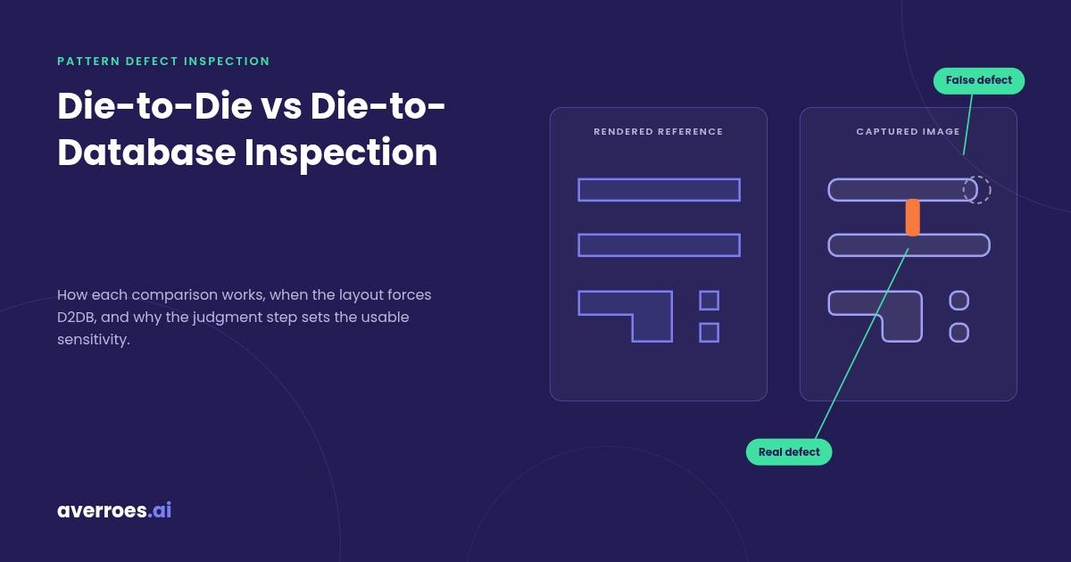
The diagram makes one point: most of what a design comparison flags is legal, and the one difference that matters looks superficially like the rest.
The cost lands on review. Set the detection threshold tight and the queue fills with corner nuisance that a human has to disposition one image at a time. Set it loose and real pattern deviations ship. The comparison engine cannot resolve this on its own, because at the pixel level a rounded corner and a real short are both differences from the reference. The usable sensitivity of die-to-database inspection is set by the judgment step, not the detection step.
That judgment is what AI automates. AI defect review from Averroes.ai compares actual against reference layout at production scale and learns, from the dispositions reviewers already make, which differences matter: a rounded corner is nuisance, a bridged line is a defect, a pulled-back line end is nuisance until it crosses the spec. Confirmed defects can then be sorted into named classes with defect classification for Pareto and feedback. The platform runs as an overlay on the mask and wafer inspection images the tools already produce, trains from 20 to 40 labeled images per class with no code, and deploys on premise so pattern data never leaves the site. The inspection tool and its comparison engine stay exactly as they are. What changes is how many of their detections deserve an engineer’s time.
Raise D2DB Sensitivity Without Flooding Review
See AI defect review on your own die-to-database inspection results
Frequently Asked Questions
What does D2DB stand for in inspection?
D2DB stands for die-to-database, the inspection comparison that checks a captured die image against a reference rendered from the design layout data. The abbreviation appears in tool specifications and SPIE literature, sometimes as D:DB, and D2DB-PM refers to die-to-database pattern monitoring on SEM images.
Is die-to-die inspection the same as die-to-die interconnect?
No. Die-to-die inspection is a defect comparison between two identically patterned dies on a mask or wafer. Die-to-die interconnect refers to the links joining chiplets inside an advanced package, as in UCIe. The terms share a name and nothing else, so tool and standard documents should be read in context.
Why do single-die reticles require die-to-database inspection?
Die-to-die comparison needs two dies with the same pattern, and a single-die reticle has only one. Large designs that fill the reticle, and development reticles that carry several differing die versions, leave the design database as the only defect-free reference available for pattern inspection.
What file formats feed the design database?
The reference starts as GDSII or OASIS layout data, the polygon formats chip designs are delivered in. The inspection tool converts the layout, maps its layers, and renders the result into the image a perfect print would produce on that tool’s optics or electron beam.
What is cell-to-cell inspection?
Cell-to-cell inspection compares each repeating cell in an array against its neighbor, most often inside memory regions. It follows the same logic as die-to-die comparison at finer grain, so it inherits the same requirement and the same blind spot: cells must be identical, and a defect repeating in every cell cancels out.
Why does die-to-database inspection produce false defects?
Because printed patterns legally deviate from drawn patterns. Corners print round, line ends pull back within specification, and OPC features make the drawing differ from the intended print by design. Each deviation is a real difference from the reference, so the comparison flags it even though nothing is wrong.







Pattern defect inspection finds printed features that deviate from their intended shape, using one of two comparisons. Die-to-die inspection compares the same pattern across two dies and flags the differences. Die-to-database inspection compares the captured image against a reference rendered from the design data itself, so it works on single-die reticles and catches defects that repeat in every die. Which one applies depends on the layout, the tool and the defect types that matter.
Pattern defect inspection sits in Stage 04 of the 12-stage semiconductor manufacturing process, and the same two comparisons run in the mask shop before a reticle ever prints. This guide from Averroes.ai, an AI visual inspection platform for manufacturers, covers how each comparison works, when each is forced, and what sets the false defect rate.
Key Notes
What Is Die-to-Database Inspection?
Die-to-database inspection is a pattern defect inspection method that compares the captured image of a die against a reference image rendered from the design data used to make it, so every deviation from design intent is detectable without a second die. The “database” is not a general-purpose database. It is the layout data for the pattern, converted and rendered into the image an ideal, defect-free die would produce on that specific tool.
That rendering step is what separates the method from every other comparison. The design exists as polygons in GDSII or OASIS layout files. An inspection tool does not see polygons. It sees an optical image blurred by its own illumination and lens, or a scanning electron microscope (SEM) image shaped by how the pattern scatters electrons. So the reference has to be computed: the tool models what its own sensor would report for a perfect print of the design, then compares that model against what the sensor actually reports.
Die-to-database inspection: from design data to defect list
Each step costs compute. Rendering a reference that faithfully models the tool, and holding alignment between a physical image and a mathematical one, is why die-to-database inspection arrived later than die-to-die comparison and why it still demands more processing behind the same scan.
The payoff is independence. The reference is the design intent itself, so the comparison answers a question die-to-die comparison cannot ask: does this pattern match what was drawn?
Die-to-Die vs Die-to-Database: When Each Applies
Die-to-die inspection compares the same pattern imaged on two neighboring dies and flags where they differ. It is an inspection comparison mode, unrelated to the die-to-die interconnects that join chiplets in advanced packaging. The method is fast and self-calibrating: both images come from the same tool in the same scan, so optics and process variation largely cancel out. Its one requirement is also its limit. There must be two dies with an identical pattern to compare.
Cell-to-cell comparison applies the same idea at finer grain. Inside memory arrays and other repeating structures, the tool compares each cell against its neighbor, which multiplies the usable references without needing a second die. The identical-pattern requirement stands, just at cell scale.
Die-to-die vs die-to-database vs cell-to-cell
The table’s sharpest row is the blind spot. A particle on a photomask prints in the same place in every die, so the two images in a die-to-die comparison carry the same flaw and the subtraction cancels it. KLA’s own patent filings on optical die-to-database inspection state the problem directly: repeating defects cannot surface in a comparison between identical repeats. Only a reference the defect is not in, the design itself, makes a repeater visible.
Layout forces the choice just as often as defect type. A reticle carrying one large die, common for GPUs and other reticle-limit designs, has no second die to compare. Development reticles often carry several differing versions of a die on purpose. Non-repeating fields have the same problem. When KLA extended its TeraScan platform’s wafer plane inspection from die-to-die to die-to-database in 2008, the drivers it named were exactly these: large single-die products and reticles without repeating structure.
In production the two modes are complements, not rivals. Tools run die-to-die comparison wherever the layout allows it, because it is cheap and robust, and die-to-database where the layout rules it out or a repeater question has to be answered. Wafer inspection programs layer both over the same hardware.
Where Die-to-Database Inspection Runs
Die-to-database inspection runs at two points in the lifecycle: in the mask shop, where it is the production standard for qualifying reticle patterns, and on wafers, where SEM-based D2DB monitors how printed patterns deviate from design.
The mask shop came first, and necessity drove it. A photomask is the master copy, a defect on it prints into every exposure, and many masks offer no second die for comparison. Optical die-to-database inspection has been the qualification standard there for decades, with effective sensitivity of roughly 50 to 60 nm defect size under production throughput conditions, as the photomask inspection guide covers across the full gate sequence. A 2023 SPIE paper on the first die-to-database flow on the MATRICS platform, presented with examples from an Intel mask shop, lists what the flow still demands today: resolution to resolve the pattern, compute for data preparation and rendering, and detection algorithms that separate real defects from background variation.
On wafers, die-to-database inspection took decades longer to become practical, and the reason is the subject of the next section: printed patterns legally deviate from their drawn shapes, so a naive comparison against design drowns in differences. What made it workable is scoping. Full-wafer optical D2DB remains rare, but SEM-based die-to-database pattern monitoring, often shortened to D2DB-PM, reuses the review and CD-SEM images a fab already collects and evaluates printed shape and critical dimension against the design at sampled sites. A 2019 SPIE paper reported the approach catching critical pattern deviations at after-develop and after-etch inspection points that conventional wafer inspection tools missed, by processing large volumes of existing SEM images rather than adding scan time. At the develop gate this runs beside post-develop inspection, where the wafer is still reworkable and a caught deviation costs a strip and recoat instead of a scrapped lot.
The division of labor is clean. Mask D2DB qualifies the master copy before it prints. Wafer D2DB-PM watches how the print itself drifts from design as the process integrates, using e-beam inspection imagery that exists anyway.
The False Defect Problem, and Where AI Review Fits
A false defect in die-to-database inspection is a flagged difference between the printed pattern and the design that is not a real defect, created because real patterns legally deviate from their drawn shapes. This is the method’s structural cost, and it is why wafer-side D2DB lagged mask-side D2DB by decades.
The deviations are not process failures. They are physics and intent. Corners draw square and print round, so every corner in the field differs from its reference. Line ends pull back within specification. Optical proximity correction (OPC) decorates the design with features that exist precisely so the print matches intent rather than the drawing, which guarantees the drawing and the print disagree. A Toshiba patent on pattern inspection describes the result plainly: corners that are rectangular in the design and curved on the substrate get detected as defects when they are not.
The diagram makes one point: most of what a design comparison flags is legal, and the one difference that matters looks superficially like the rest.
The cost lands on review. Set the detection threshold tight and the queue fills with corner nuisance that a human has to disposition one image at a time. Set it loose and real pattern deviations ship. The comparison engine cannot resolve this on its own, because at the pixel level a rounded corner and a real short are both differences from the reference. The usable sensitivity of die-to-database inspection is set by the judgment step, not the detection step.
That judgment is what AI automates. AI defect review from Averroes.ai compares actual against reference layout at production scale and learns, from the dispositions reviewers already make, which differences matter: a rounded corner is nuisance, a bridged line is a defect, a pulled-back line end is nuisance until it crosses the spec. Confirmed defects can then be sorted into named classes with defect classification for Pareto and feedback. The platform runs as an overlay on the mask and wafer inspection images the tools already produce, trains from 20 to 40 labeled images per class with no code, and deploys on premise so pattern data never leaves the site. The inspection tool and its comparison engine stay exactly as they are. What changes is how many of their detections deserve an engineer’s time.
Raise D2DB Sensitivity Without Flooding Review
See AI defect review on your own die-to-database inspection results
Frequently Asked Questions
What does D2DB stand for in inspection?
D2DB stands for die-to-database, the inspection comparison that checks a captured die image against a reference rendered from the design layout data. The abbreviation appears in tool specifications and SPIE literature, sometimes as D:DB, and D2DB-PM refers to die-to-database pattern monitoring on SEM images.
Is die-to-die inspection the same as die-to-die interconnect?
No. Die-to-die inspection is a defect comparison between two identically patterned dies on a mask or wafer. Die-to-die interconnect refers to the links joining chiplets inside an advanced package, as in UCIe. The terms share a name and nothing else, so tool and standard documents should be read in context.
Why do single-die reticles require die-to-database inspection?
Die-to-die comparison needs two dies with the same pattern, and a single-die reticle has only one. Large designs that fill the reticle, and development reticles that carry several differing die versions, leave the design database as the only defect-free reference available for pattern inspection.
What file formats feed the design database?
The reference starts as GDSII or OASIS layout data, the polygon formats chip designs are delivered in. The inspection tool converts the layout, maps its layers, and renders the result into the image a perfect print would produce on that tool’s optics or electron beam.
What is cell-to-cell inspection?
Cell-to-cell inspection compares each repeating cell in an array against its neighbor, most often inside memory regions. It follows the same logic as die-to-die comparison at finer grain, so it inherits the same requirement and the same blind spot: cells must be identical, and a defect repeating in every cell cancels out.
Why does die-to-database inspection produce false defects?
Because printed patterns legally deviate from drawn patterns. Corners print round, line ends pull back within specification, and OPC features make the drawing differ from the intended print by design. Each deviation is a real difference from the reference, so the comparison flags it even though nothing is wrong.