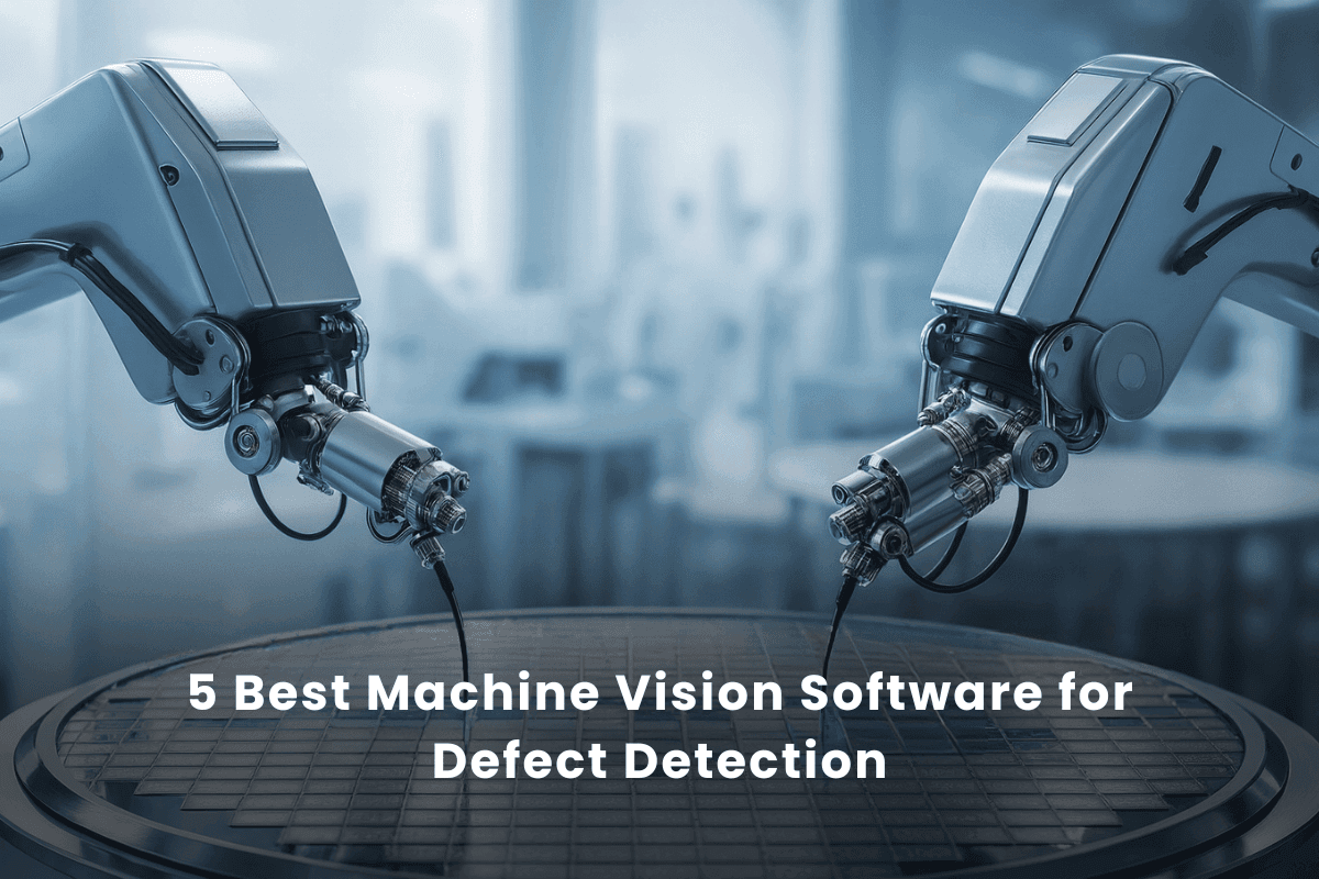
5 Best Machine Vision Software for Defect Detection 2026
Averroes
May 18, 2026
The best machine vision software for defect detection has a widening gap between adaptive AI platforms and the legacy systems holding manufacturers back.
Some rely on template matching and constant recalibration. Others use adaptive AI that catches defects no one even labeled yet.
Add in questions of speed, accuracy, and hardware, and the choice isn’t simple.
We’ll break down the best machine vision software for defect detection in 2026 – what each does well, and where each falls short.
Our Top 3 Picks
Best for Complete Accuracy and Adaptability Across Industries
Best Overall Machine Vision Software for Accuracy and Ease of Use
We’re putting Averroes first on this list – not just because it’s our own platform, but because the feedback we hear from users consistently places it among the strongest options for defect detection in high-precision manufacturing.
Unlike older systems that rely on template matching or struggle with unknown defects, Averroes uses unsupervised learning to catch both known and emerging anomalies with 99%+ accuracy.
It integrates seamlessly with existing hardware, offers flexible deployment options, and supports defect classification, segmentation, and review across industries from semiconductors and solar to pharma, food and beverage, and even oil and gas.
While it remains a software-only solution that pairs with compatible cameras, users report measurable gains in speed, yield, and inspection efficiency.
Features
No-code AI model creation in hours, not weeks
WatchDog anomaly detection for unknown defects
Data-agnostic and integrates with existing inspection hardware
Continuous learning and active feedback adaptation
High-precision defect detection at submicron and nanometer scale
Pros:
99%+ Accuracy: Near-zero false rejects
Enhanced Performance: Increases defect detection rates by ~60% and yield by up to 20%
Time Savings: Saves 300+ labor hours per application each month
Flexible Deployment: Options for cloud or on-premises setup
Industry Proven: Strong performance in high-precision sectors like semiconductors
Cons:
System Requirements: Requires existing compatible cameras and automation setup
Cognex is one of the most established names in machine vision, and the In-Sight 2800 shows why. It combines AI-driven edge learning with traditional rule-based tools, giving manufacturers flexibility to tackle everything from simple presence/absence checks to more advanced defect classification and OCR.
Reviews often mention its intuitive EasyBuilder setup, reliable imaging quality with HDR technology, and the ability to scale with modular components.
While some engineers compare it against Keyence for software preference or specific project fit, Cognex remains a go-to option for consistent, reliable vision applications across industries.
Features
Hybrid AI + rule-based vision system
EasyBuilder development environment for rapid deployment
OCR that reads low-contrast or reflective surfaces
HDR imaging for 16x detail compared to standard sensors
Modular hardware with flexible lighting options
Pros:
Reliable & Widely Adopted: Strong industry reputation with proven track record
User-Friendly Setup: Step-by-step guidance for easy implementation
Unlimited Classification: Multi-feature inspection outputs available
Good Resolution & Field of View: Suitable for varied applications
Strong Support Ecosystem: Comprehensive training and support available
Cons:
Limited Spreadsheet Interface: Advanced features only available on certain models
High Upfront Cost: Significant initial investment required
Best for High-Speed 3D Automated Optical Inspection (AOI)
Mirtec has built its reputation around optical inspection, and its AOI systems – especially the MV-6 OMNI – are often highlighted for their strong 3D capabilities.
Using OMNI-VISION® technology with multi-frequency Moiré projection, Mirtec machines deliver precise defect detection at sub-second speeds, making them well-suited for high-volume electronics production.
Reviews consistently point out the clear, noise-free 3D imaging, fast throughput, and dependable performance in demanding environments. On the flip side, the machines are physically large and sometimes require skilled setup for advanced features, but for manufacturers prioritizing speed and accuracy, Mirtec is a proven option.
Features
OMNI-VISION® 3D inspection with multi-pattern Moiré projection
High-resolution center + angled cameras for full-surface visibility
Fast inspection (~0.77 sec per spot) with turbo mode up to 45% faster
8-phase coaxial color lighting for reflective components and microcracks
Auto Fine Tuning for simpler setup and consistent results
Pros:
High-Quality Imaging: Clear, high-quality 3D imaging with strong defect detection
High-Speed Processing: High-speed inspections for high-volume lines
Reliable Results: Reliable and repeatable results, even in complex environments
User-Friendly: User-friendly interface with auto-optimization
Global Support: Good global support network
Cons:
Large Footprint: Large system footprint may limit installation flexibility
KLA, through its Orbotech line, is widely seen as a leader in semiconductor and PCB inspection. Its systems are engineered for precision at the micrometer and even nanometer scale, combining optical and e-beam technologies with AI-driven algorithms.
Reviews highlight the ability to catch defects on patterned and unpatterned wafers, PCBs, and advanced nodes down to ≤5nm. Features like Multi-Image™ and SIP™ technologies help minimize false rejects while boosting throughput, making KLA a standard in fabs and advanced electronics production.
The trade-offs are significant: calibration requirements and very high upfront costs.
Features
Multi-Image™ and SIP™ technology for high detection with fewer false rejects
AI- and ML-driven classification for faster root cause analysis
Compatible with patterned/unpatterned wafer inspection, PCB, and semiconductor lines
Inline monitoring with optical + e-beam inspection
Real-time defect data analysis and integration into production lines
Pros:
Extremely high accuracy: at nanometer and micrometer scale
Strong suite of capabilities: AOI + metrology capabilities
Effective yield optimization: through low false reject rates
Proven in advanced nodes: (≤5nm logic, DRAM, NAND)
Cons:
Calibration required: tuning needed to minimize false alarms
Scale limitation: best suited for large fabs, not smaller manufacturers
Camtek has long been a fixture in semiconductor inspection, with systems like Eagle, Falcon, and Gryphon widely used in fabs.
Its Automatic Defect Classification (ADC) software is dependable for catching common, repeatable defects through template matching, and users often highlight the strong support and training that comes with it.
Where it falls short is in adaptability. Unlike AI-native platforms, Camtek requires manual calibration and updates, making it less effective against unknown or complex defect types. Reviewers note higher false reject rates and slower responsiveness to new challenges.
For fabs with stable, well-understood defect profiles, though, Camtek remains a reliable option.
Features
Image-based automatic defect classification (ADC)
Built-in setup tools for re-training and qualification
Flexible classification engine for standardized data
Strong support and training ecosystem
Pros:
Reliable for consistent, known defect types: Performs well with familiar defect patterns
Well-suited for repetitive inspection processes: Optimized for consistent workflows
Backed by strong service and global support: Comprehensive customer assistance worldwide
Solid track record in semiconductor fabs: Proven performance in manufacturing environments
Cons:
High false reject rates on complex or unknown defects: Struggles with unfamiliar or intricate defect patterns
Requires frequent calibration and expert intervention: Needs ongoing maintenance and specialist expertise
No continuous learning – adaptability limited to software updates: Cannot self-improve or adapt without manual updates
Comparison: Best Machine Vision Software for Defect Detection
Feature / Capability
Averroes.ai
Cognex
Mirtec
KLA
Camtek
High Precision
✔️
✔️
✔️
✔️
❌
Detects Unknown Defects
✔️
❌
❌
❌
❌
Continuous Learning / Adaptability
✔️
⚠️
❌
⚠️
❌
No-Code / Easy Setup
✔️
✔️
✔️
❌
❌
Hardware Offerings
❌
✔️
✔️
✔️
✔️
Multi-Industry Use
✔️
✔️
❌
❌
❌
Low False Reject Rate
✔️
✔️
✔️
✔️
❌
How To Choose The Best Machine Vision Software For Defect Detection?
Choosing the best machine vision software for defect detection comes down to more than just accuracy claims. You’ll want to weigh how well the software aligns with your production environment, industry, and long-term goals.
Here are the key criteria – and how the five options stack up:
1. Accuracy and Precision Requirements
If your process demands submicron or nanometer-level machine vision defect detection, accuracy is non-negotiable. Semiconductor fabs and advanced electronics lines fall squarely in this category.
Stronger options: Averroes.ai (99%+ accuracy with continuous learning) and KLA (high precision at ≤5nm nodes).
Less strong: Camtek, which works reliably for known defect types but struggles with complex or unknown anomalies.
2. Ability to Detect Unknown Defects
Many systems can flag known, repeatable defects. But in dynamic environments, you need software that can adapt.
Stronger options: Averroes.ai stands out here with unsupervised learning that captures both known and unknown defects.
Less strong: Camtek (template matching only) and Mirtec (excellent speed and imaging, but relies on predefined profiles).
3. Ease of Deployment and Setup
Complex inspection shouldn’t require months of onboarding or a team of specialists.
Stronger options: Averroes.ai (no-code deployment) and Cognex (EasyBuilder step-by-step setup).
Less strong: KLA and Mirtec, which require skilled setup and are more suited to large fabs with dedicated engineering support.
4. Hardware vs. Software Flexibility
Decide if you want a turnkey solution (hardware + software) or software that layers onto your existing equipment.
Software-first flexibility: Averroes.ai integrates with existing cameras and infrastructure, minimizing capital spend.
Hardware-bound systems: Cognex, Mirtec, KLA, and Camtek all package hardware with their software, which can increase cost but may appeal to buyers wanting a single-vendor solution.
5. Speed and Throughput
Production speed matters – inspection software should keep pace without bottlenecks.
High-speed leaders: Mirtec (sub-second inspection with turbo mode) and KLA (fab-level throughput).
Balanced: Averroes.ai, which delivers scalable software speed without large machine footprints.
Less strong: Camtek, where frequent calibration can slow operations.
6. Industry Versatility
The best machine vision software adapts across sectors rather than being narrowly designed for one.
Most versatile: Averroes.ai, proven in semiconductors, electronics, pharma, food & beverage, solar, and even oil & gas with drone inspection.
Broader but still niche: Cognex (good for electronics, packaging, automotive) and Mirtec (electronics-focused).
Narrowest: KLA and Camtek, largely limited to semiconductors and PCB manufacturing.
7. Cost and ROI
Upfront cost and long-term return both matter. A system that saves labor hours or boosts yield often pays for itself quickly.
Cost-efficient with high ROI: Averroes.ai (software-only, saves 300+ labor hours per application monthly).
Higher cost but justified in fabs: KLA and Mirtec.
Expensive relative to flexibility: Camtek, especially given its limited adaptability.
Catch Every Defect – Known And Unknown
Works with any existing hardware, including those in this list.
Best Machine Vision Software For Defect Detection FAQs
What’s the difference between machine vision software and hardware-based inspection systems?
Machine vision software focuses on algorithms and AI models that analyze images, while hardware-based systems bundle in cameras, lighting, and processors. Software-only solutions integrate with existing equipment, whereas hardware bundles may increase cost but simplify vendor management.
Can machine vision software integrate with legacy production lines?
Yes, many platforms (like Averroes.ai) are designed to work with existing cameras and automation infrastructure. Others may require proprietary hardware or upgrades, so compatibility should be confirmed before purchase.
How much training data is needed to build an accurate defect detection model?
This varies widely. Traditional systems may need thousands of images, while AI-driven platforms can start with as few as 20–40 images per defect class and improve continuously over time.
Does machine vision software require constant recalibration?
Not always. AI-powered systems with continuous learning adapt automatically to new defect patterns, reducing the need for recalibration. Older or template-based platforms often require more frequent manual adjustments.
Conclusion
Finding the best machine vision software for defect detection comes down to matching the tool with your production needs.
Some platforms, like Cognex, stand out for flexible rule-based and AI inspection. Mirtec is a strong pick for high-speed 3D AOI in electronics, while KLA remains the heavyweight for advanced node wafer inspection in large fabs. Camtek fits manufacturers with established, repetitive defect profiles.
Averroes, though, combines adaptability, accuracy, and scalability – catching both known and unknown defects across industries from semiconductors to pharma, food and beverage, and solar.
If you’re looking to reduce false rejects, save hundreds of hours, and run defect detection on existing hardware, book a free demo of Averroes today and see how it fits into your production goals.


The best machine vision software for defect detection has a widening gap between adaptive AI platforms and the legacy systems holding manufacturers back.
Some rely on template matching and constant recalibration. Others use adaptive AI that catches defects no one even labeled yet.
Add in questions of speed, accuracy, and hardware, and the choice isn’t simple.
We’ll break down the best machine vision software for defect detection in 2026 – what each does well, and where each falls short.
Our Top 3 Picks
Best for Complete Accuracy and Adaptability Across Industries
Averroes.ai
VIEW NOWBest for High-Speed 3D AOI in Electronics
Mirtec
VIEW NOWBest for Advanced Node Wafer Inspection in Fabs
KLA
VIEW NOW1. Averroes.ai
Best Overall Machine Vision Software for Accuracy and Ease of Use
We’re putting Averroes first on this list – not just because it’s our own platform, but because the feedback we hear from users consistently places it among the strongest options for defect detection in high-precision manufacturing.
Unlike older systems that rely on template matching or struggle with unknown defects, Averroes uses unsupervised learning to catch both known and emerging anomalies with 99%+ accuracy.
It integrates seamlessly with existing hardware, offers flexible deployment options, and supports defect classification, segmentation, and review across industries from semiconductors and solar to pharma, food and beverage, and even oil and gas.
While it remains a software-only solution that pairs with compatible cameras, users report measurable gains in speed, yield, and inspection efficiency.
Features
Pros:
Cons:
Score: 4.8/5
View Now
2. Cognex In-Sight 2800
Best for Versatile Rule-Based + AI Inspection
Cognex is one of the most established names in machine vision, and the In-Sight 2800 shows why. It combines AI-driven edge learning with traditional rule-based tools, giving manufacturers flexibility to tackle everything from simple presence/absence checks to more advanced defect classification and OCR.
Reviews often mention its intuitive EasyBuilder setup, reliable imaging quality with HDR technology, and the ability to scale with modular components.
While some engineers compare it against Keyence for software preference or specific project fit, Cognex remains a go-to option for consistent, reliable vision applications across industries.
Features
Pros:
Cons:
Score: 4.6/5
View Now
3. Mirtec AOI Systems
Best for High-Speed 3D Automated Optical Inspection (AOI)
Mirtec has built its reputation around optical inspection, and its AOI systems – especially the MV-6 OMNI – are often highlighted for their strong 3D capabilities.
Using OMNI-VISION® technology with multi-frequency Moiré projection, Mirtec machines deliver precise defect detection at sub-second speeds, making them well-suited for high-volume electronics production.
Reviews consistently point out the clear, noise-free 3D imaging, fast throughput, and dependable performance in demanding environments. On the flip side, the machines are physically large and sometimes require skilled setup for advanced features, but for manufacturers prioritizing speed and accuracy, Mirtec is a proven option.
Features
Pros:
Cons:
Score: 4.4/5
View Now
4. KLA (Orbotech)
Best-in-Class for Advanced Node Wafer Inspection
KLA, through its Orbotech line, is widely seen as a leader in semiconductor and PCB inspection. Its systems are engineered for precision at the micrometer and even nanometer scale, combining optical and e-beam technologies with AI-driven algorithms.
Reviews highlight the ability to catch defects on patterned and unpatterned wafers, PCBs, and advanced nodes down to ≤5nm. Features like Multi-Image™ and SIP™ technologies help minimize false rejects while boosting throughput, making KLA a standard in fabs and advanced electronics production.
The trade-offs are significant: calibration requirements and very high upfront costs.
Features
Pros:
Cons:
Score: 4.1/5
View Now
5. Camtek
Best for Established, Known Defect Profiles
Camtek has long been a fixture in semiconductor inspection, with systems like Eagle, Falcon, and Gryphon widely used in fabs.
Its Automatic Defect Classification (ADC) software is dependable for catching common, repeatable defects through template matching, and users often highlight the strong support and training that comes with it.
Where it falls short is in adaptability. Unlike AI-native platforms, Camtek requires manual calibration and updates, making it less effective against unknown or complex defect types. Reviewers note higher false reject rates and slower responsiveness to new challenges.
For fabs with stable, well-understood defect profiles, though, Camtek remains a reliable option.
Features
Pros:
Cons:
Score: 4.0/5
View Now
Comparison: Best Machine Vision Software for Defect Detection
How To Choose The Best Machine Vision Software For Defect Detection?
Choosing the best machine vision software for defect detection comes down to more than just accuracy claims. You’ll want to weigh how well the software aligns with your production environment, industry, and long-term goals.
Here are the key criteria – and how the five options stack up:
1. Accuracy and Precision Requirements
If your process demands submicron or nanometer-level machine vision defect detection, accuracy is non-negotiable. Semiconductor fabs and advanced electronics lines fall squarely in this category.
2. Ability to Detect Unknown Defects
Many systems can flag known, repeatable defects. But in dynamic environments, you need software that can adapt.
3. Ease of Deployment and Setup
Complex inspection shouldn’t require months of onboarding or a team of specialists.
4. Hardware vs. Software Flexibility
Decide if you want a turnkey solution (hardware + software) or software that layers onto your existing equipment.
5. Speed and Throughput
Production speed matters – inspection software should keep pace without bottlenecks.
6. Industry Versatility
The best machine vision software adapts across sectors rather than being narrowly designed for one.
7. Cost and ROI
Upfront cost and long-term return both matter. A system that saves labor hours or boosts yield often pays for itself quickly.
Catch Every Defect – Known And Unknown
Works with any existing hardware, including those in this list.
Best Machine Vision Software For Defect Detection FAQs
What’s the difference between machine vision software and hardware-based inspection systems?
Machine vision software focuses on algorithms and AI models that analyze images, while hardware-based systems bundle in cameras, lighting, and processors. Software-only solutions integrate with existing equipment, whereas hardware bundles may increase cost but simplify vendor management.
Can machine vision software integrate with legacy production lines?
Yes, many platforms (like Averroes.ai) are designed to work with existing cameras and automation infrastructure. Others may require proprietary hardware or upgrades, so compatibility should be confirmed before purchase.
How much training data is needed to build an accurate defect detection model?
This varies widely. Traditional systems may need thousands of images, while AI-driven platforms can start with as few as 20–40 images per defect class and improve continuously over time.
Does machine vision software require constant recalibration?
Not always. AI-powered systems with continuous learning adapt automatically to new defect patterns, reducing the need for recalibration. Older or template-based platforms often require more frequent manual adjustments.
Conclusion
Finding the best machine vision software for defect detection comes down to matching the tool with your production needs.
Some platforms, like Cognex, stand out for flexible rule-based and AI inspection. Mirtec is a strong pick for high-speed 3D AOI in electronics, while KLA remains the heavyweight for advanced node wafer inspection in large fabs. Camtek fits manufacturers with established, repetitive defect profiles.
Averroes, though, combines adaptability, accuracy, and scalability – catching both known and unknown defects across industries from semiconductors to pharma, food and beverage, and solar.
If you’re looking to reduce false rejects, save hundreds of hours, and run defect detection on existing hardware, book a free demo of Averroes today and see how it fits into your production goals.