AOI are studied. Let's Smarten them up.

Automated Optical Inspection Systems with AI

Deep learning-powered automated optical inspection that achieves 99%+ accuracy, adapts to your production line, and gets smarter over time—without calibration, domain experts, or million-dollar AOI machine investments.

analytics model Image

The Cost of AOI Failures in Semiconductor Manufacturing

Traditional AOI systems create critical operational challenges that directly impact your bottom line

False Rejects
Good products flagged as defective due to template matching sensitivity
15-40% of flagged defects are false alarms
Unnecessary scrap and rework costs
Manual review bottlenecks production
Misclassification
Defects categorized incorrectly by legacy automated optical inspection equipment, masking root causes
Unable to identify true defect patterns
Delayed response to process issues
Lost opportunities for yield improvement
Escapees
Real defects missed by traditional AOI machines and shipped to customers
Customer returns and warranty claims
Reputation damage and lost contracts
Regulatory compliance risks
The Combined Impact
These AOI failures cost semiconductor manufacturers millions annually in lost yield, manual review labor, customer returns, and missed process improvement opportunities. Traditional template-based systems simply cannot adapt to the complexity of modern semiconductor manufacturing.

How Averroes.ai Solves Each Challenge

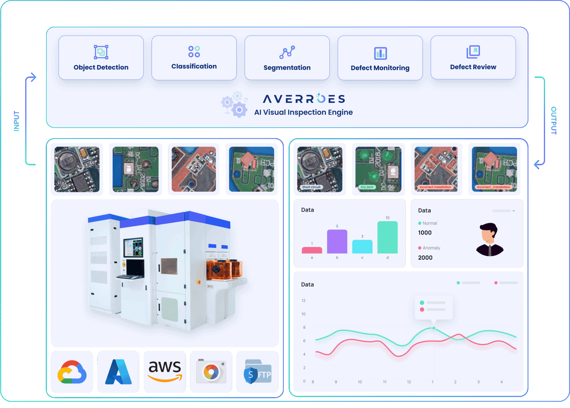
Deep learning models tailored to your specific defect types and automated optical inspection workflow

Near-Zero False Rejects

Our deep learning classification and detection models power AI AOI, achieving 99%+ accuracy and virtually eliminating false alarms that waste good products.

Smart augmentation trains on diverse scenarios
Adapts to natural process variation
Reduces manual review by up to 90%
Traditional AOI
60-85% accuracy
Averroes.ai
99%+ accuracy
Defect Type: Scratch
98%
Defect Type: Particle
99%
Defect Type: Stain
97%

Precise Classification

Advanced detection models accurately classify defect types with 99%+ precision, enabling targeted root cause analysis and process improvements across automated optical inspection systems.

Multi-class detection for complex defects
Identify true failure modes faster
Accelerate yield improvement initiatives

Zero Escapees

High-sensitivity detection models catch even the most subtle defects with 99%+ recall, ensuring defective products never reach your customers.

Detects micro-defects invisible to traditional AOI
Continuous learning improves detection over time
Protect brand reputation and customer relationships
99.8%
Defect Detection Rate
Protects quality while maintaining high throughput

From Implementation to Continuous Improvement

A proven process that delivers results in weeks, not months

Step 1
Collect Your Data
We work with your existing automated optical inspection system to gather historical inspection images and defect labels. No production disruption—we use your current data.
Typical dataset: 1,000-5,000 images (30-40 per defect class)
Works with all major AOI formats
Data collection: 1-2 weeks
Step 2
Train Custom Models
Our AI engineers build classification and detection models specifically trained on your defect types, augmented with smart techniques to handle edge cases.
State-of-the-art deep learning architectures
Smart augmentation for robustness
Training & validation: 2-3 weeks
Step 3
Deploy On-Premise
Models are deployed directly to your facility with secure, air-gapped infrastructure. Your data never leaves your premises. Seamless integration with existing systems.
Complete data sovereignty
Low-latency real-time inference
Deployment & testing: 1 week
Step 4
Improve Over Time
Active Learning continuously identifies edge cases and retrains models with new data. Your system gets smarter with every production run—no manual tuning required.
Automatic edge case detection
Periodic model updates & retraining
Performance analytics dashboard
Total Time to Production
4-6 Weeks
From data collection to live production deployment with measurable ROI

Key Platform Features

Maximizing Operational Excellence and Asset Reliability

95% Nuisance Reduction

Reduce nuisance detection rate from 40-70% down to 5-10%, eliminating false alarms while maintaining 95-99% DOI capture. Break the traditional trade-off between sensitivity and accuracy.

90% Review Time Savings

Cut lot dispositioning time from 30-60 minutes to just 3-5 minutes. Reduce weekly engineer review hours by 85-90%, freeing your team to focus on value-add problem solving instead of triage.

2-5% Yield Recovery

Recover millions in annual yield by eliminating false scraps and unnecessary rework caused by legacy automated optical inspection machines. For a 200mm fab, achieve $5-15M in annual value with 7-9 day payback period and 38-51x ROI.

Continuous Active Learning

AI models improve 2-3% per week during first month. Automatically adapt to process drift, equipment changes, and new defect types with just 10-20 examples vs. 100+ for traditional ML.

2-3 Week Deployment

Zero disruption, zero hardware changes. Ingest images via SECS/GEM, E84, or network shares. Deploy in shadow mode initially, transition gradually as confidence builds. Full production in weeks, not months.

Early Excursion Detection

Detect systematic defects and process drift 2- 4 lots earlier than traditional SPC. Real-time alert system with detailed root cause analysis enables fast, informed responses to prevent yield loss.
Frequently asked questions
Typical results across semiconductor fabs: +2-5% absolute probe yield improvement from eliminating false scraps, recovered 30-80 additional good die per wafer, 70-85% reduction in unnecessary scraps and reworks, and 60-75% reduction in defective wafer volume from excursion impact.

Experience the AI Inspection Advantage

Elevate Your Visual Inspection Capabilities
See measurable nuisance reduction, DOI validation, and full ROI analysis in 6 weeks